Integrated photonic platforms - The case for SiC
The potential of SiC integrated photonics is starting to be unleashed, thanks to the unique photonic properties of this material and the development of high-quality epitaxial growth.
BY HAIYAN OU FROM THE TECHNICAL UNIVERSITY OF DENMARK
The most mature and applied semiconductor ever, silicon, is the pillar for modern microelectronics. For the last 50 years or more it has been revolutionising human life, with progress in computation prowess spurred on by adherence to Moore Law, leveraging planar processing.
However, the shrinking of device dimensions cannot continue forever. Line widths are now approaching their physical limit, leading those at the forefront of this technology to search for a way forward to address the looming bottleneck. One promising option involves turning to integrated photonics.
Electrons versus photons
A crucial difference between integrated electronics and integrated photonics is the carrier. Evaluated in this regard, the latter has much appeal. The merits of the photon include: an absence of charge, preventing interference from electromagnetic fields; and an absence of mass, enabling devices to operate at far faster speeds than their electronic counterparts (see Table 1). However, there are challenges in the photonic domain, including the manipulation of this carrier.
In integrated electronics, silicon dominates. Meanwhile, in integrated photonics multiple material platforms co-exist, including silicon, Si3N4, GaAs, InP, GaP, AlN, LiNbO3 and SiC. This high level of diversity reflects the fact that no single material provides the six basic building blocks for an integrated photonic chip: a light source, a waveguide, a modulator, detection, low-cost assembly and intelligence.
Silicon is playing a very active role in photonics, thanks to a well-developed material and its mature processing, refined over many decades of manufacture of integrated electronics. However, silicon has two significant drawbacks. The first is that it is an indirect bandgap semiconductor, so is inherently inefficient for light emission; and the second is that due to a bandgap of 1.12 eV, strong two-photon absorption occurs at telecommunication wavelengths, screening other nonlinearities, such as four-wave mixing, which provides wavelength conversion.
These two restraints create opportunities for other materials, such as III-Vs and wide bandgap semiconductors. For example, direct bandgap III-V semiconductors are ideal for integrated lasers solutions, while wide bandgap semiconductors have negligible two-photon-absorption within the telecommunication wavelength range.

Table 1. Comparison of photons and electrons
SiC: Pros and cons
Within this family of compound semiconductors, SiC is emerging as a very promising candidate for integrated photonics. This wide bandgap material has many strengths, including being CMOS compatible, bio-compatible, abundant, non-toxic and thus sustainable; and it has unique photonic properties, such as both high second-order and third-order nonlinearities, a high refractive index, a wide bandgap, and a low intrinsic material loss. Additional strengths include having more than 250 polytypes with variable properties, a thermal conductivity that’s more than three times that of silicon, and stable mechanical, physical and chemical characteristics. Furthermore, the processing of SiC is advanced – there is a mature growth technology for producing high crystal-quality SiC, engineers know how to dope this material, and mature material growth and device fabrication has already been established for SiC power electronics, laying the foundation for efforts to scale SiC in integrated photonics.
The wide adoption of SiC power devices, particular in electric vehicles, has laid a solid foundation for the deployment of this material system in SiC photonics. However, despite these advances in materials and fabrication, three substantial challenges have to be addressed: the formation of SiC-on-insulator (SiCOI) stacks, in order to confine the light in SiC; the development of nanofabrication technology, for low loss and dispersion control; and the introduction of an efficient coupling scheme for the coupling of light in and out of a chip.
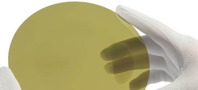
In photonic circuits, the path of the photon is controlled by the waveguide, using total internal reflection to steer light through the structure. To ensure that photons are confined within a SiC layer, this material is embedded in low refractive index material, such as SiO2. Commercially available SiC tends to be in the form of wafers, typically 500 mm-thick, while the SiC layer in a SiCOI stack is normally less than 1 µm.
The first big challenge to address is to transfer SiC from a wafer to a thin layer. Our team at the Technical University of Denmark initially took on this challenge with an ion-cut method, also known as smart cut, well established for the production of SOI wafers. Unfortunately, this approach led to a high optical loss of around 6 dB/cm, resulting from ion implantation.
This loss could not be reduced dramatically by thermal annealing, due to limitations associated with the lower melting temperature of the silicon substrate. One possible solution might be to turn to laser annealing, rather than furnace annealing, as this source can be focused to a small spot, allowing just the SiC layer to experience a high temperature for defect recovery, while maintaining the silicon substrate below its melting point.

Figure 1. The microcomb development roadmap.
Our current approach differs from this. We avoid ion implantation altogether, using a bonding and grinding method to form our SiCOI structures. However, the yield is still very low.
Another concern is waveguide loss, resulting from imperfections in fabrication. If there is any roughness at the surface of the SiC waveguide, this increases its loss. To minimise this we have optimised our SiC waveguide fabrication process, which consists of electron-beam lithography, dry etching and top-cladding SiO2 deposition. This approach enables us to form SiC waveguides with a well-defined geometry and a smooth surface.
A typical cross-sectional geometry of our SiC waveguides is around 500 nm by 500 nm. While this is much bigger than the feature size of a FET, the transistor used to control electron transport in ICs, it is still much smaller than a spot size from a standard single mode fibre – that’s around 10 mm. Due to this significant difference in size, we have devoted much effort to ensuring efficient light coupling between a standard single-mode fibre and a SiC waveguide, using mode conversion on the chip. We also aim to achieve extremely low loss within the waveguide, so that we don’t need an on-chip amplifier, a device that doesn’t exist yet.
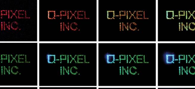
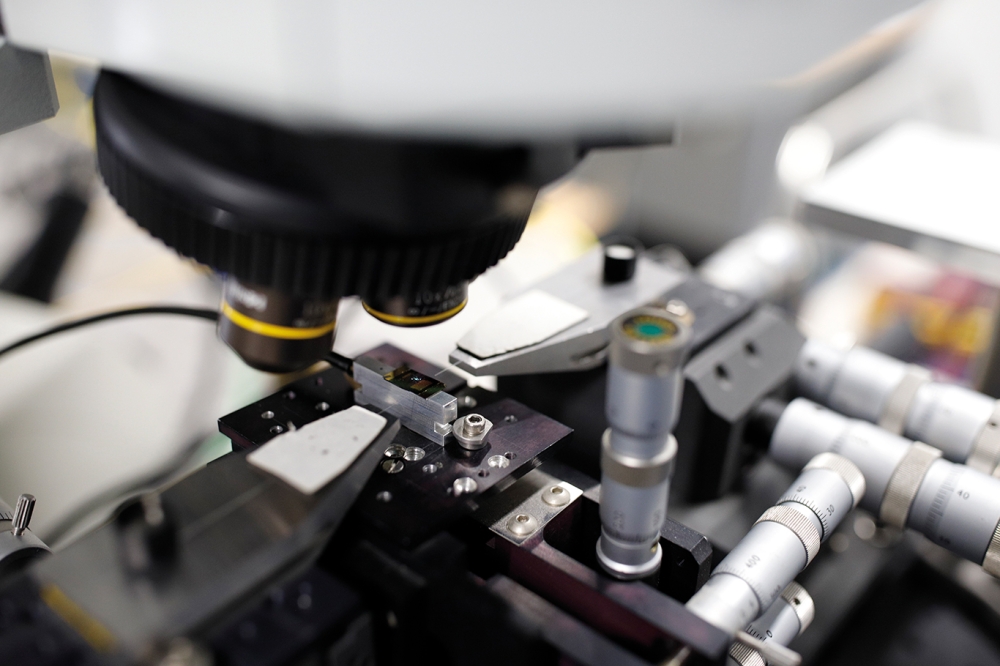
To test our SiC optical chips, we use a high magnification microscope to aid the alignment of SiC waveguides and optical fibres (see opening image). This task is supported by mounting the optical chip and the fibre ends on three-dimensional adjustable stages.

Table 2: Comparison of SiC with other material platforms in
integrated photonics.
Optical frequency combs
Back in 2005, the Nobel Prize in physics went to pioneers in the field of optics. Roy Glauber won half the award for his contribution to the quantum theory of optical coherence, and the other half was shared by John Hall and Theodor Hänsch, for their contribution to the development of laser-based precision spectroscopy, including the optical frequency comb (OFC) technique. An OFC produces a spectrum with discrete, distinct, and equally spaced frequency lines – it is like a ruler for measuring light frequencies.
The chip-scale frequency comb, also called a microcomb, represents the third generation of OFC. It follows the mode-locked laser OFC, the first generation of this technology, and the more recent fibre laser OFC, the second generation of this technology. Combining the advances of nanofabrication and nonlinear optics, the microcomb is attracting much interest. It’s now a very hot research topic, due to strengths that include the compactness of the OFC, its efficiency, its ultra-wide band output, and its potential to serve in a wide range of applications. Microcombs could be used for spectroscopy, optical communication, metrology, optical atomic clocks, bio/chemical sensing, distance ranging and searching for exoplanets.
Progress with microcombs has propelled them to an advanced state called the octave and dissipative Kerr soliton, which realises self-reference and coherence. Thanks to the highly compact geometry, comb tooth spacings can now be in the range of tens of gigahertz to terahertz, further expanding the application range of traditional mode-locked laser combs.
Among the different material platforms that can be considered for photonic integration (see Table 2), SiC is one that is going to open a door to new optical devices, including microcombs, thanks to its unique optical properties. Its strengths include a wide bandgap, and high second-order and third order optical nonlinearity.
Due to its wide bandgap, frequency comb light sources based on SiC can cover an ultra-wide band from near ultraviolet to mid-infrared. Within this wide spectral domain disinfection, lighting, communication, biosensing and gas sensing all have individual footprints, some of which are yet to be covered by standard lasers. The high second-order and third-order non-linearity of SiC are advantageous, because they make the SiC frequency comb energy efficient and broad.
There are also significant opportunities for the SiC OFC in the likes of quantum optics and quantum networks, quantum computing, sensing, and imaging. This technology is sure to make an impact, enabling more secure and scalable integrated quantum networks, and possibly new embedded biosensors that revolutionise medical diagnosis, thanks to the biocompatibility of SiC material.

Figure 2. SiCOI OFC generated from a microring resonator.
Over the last 10 years much progress has been made in chip-scale OFCs, also known as microcombs (see Figure 1 for a brief development roadmap since 2014). Key breakthroughs include the demonstration of chip-scale OFCs using MgF2 in 2014, SiO2 in 2015, Si3N4 in 2017, both AlGaAs and Hydex silica in 2018, LiNbO3 in 2019, GaP in 2020, both Ta2O5 and SiC in 2021, and GaN in 2022.
Aside from LiNbO3, which generates an OFC through second-order nonlinearity (an electro-optic comb), the rest of the OFCs are realised through a third-order nonlinearity, and are known as a Kerr comb. Of these, Si3N4 is marked with an octave dissipative Kerr soliton, and provides a fully stable OFC. LiNbO3, SiC, GaN and AlN are marked to have second-order nonlinearity. Unlike materials without second-order nonlinearity, these four have the capability to realise an octave bandwidth through wavelength conversion via frequency doubling. Despite the late arrival of SiC to OFCs, this material has caught up, demonstrating its capability and showcasing its tremendous potential in photonics, due to a nanofabrication-friendly nature and unique optical properties. Illustrating this point is a Kerr comb generated from a SiCOI microring resonator, shown in Figure 2.
Pioneering SiC OFCs
Our team is a trailblazer of SiC OFC technology, realising a number of important milestones over the last few years. In 2019 we reported the first integrated SiC microring resonator from 4H SiCOI made by the ion-cut method, as well as demonstrating four-wave mixing and deriving a non-linear refractive index for 4H SiCOI. A year later we demonstrated supercontinuum generation from 4H SiCOI waveguides made by the ion-cut method, and in 2021 we announced optical parametric oscillation from 4H SiCOI made by the ion-cut method. Further breakthroughs have followed in the last few years. In 2022 we demonstrated a 4H SiCOI beam splitter, polarisation beam splitter and Mach-Zehnder interferometer, and filed a patent for fabricating 4H SiCOI material stacks. And in 2023 we demonstrated: a 4H SiCOI polarisation and mode multiplexer; OFC from 4H SiCOI; and four-wave mixing from amorphous SiCOI, as well as deriving the non-linear refractive index for this particular material.
SiC is now attracting intensive interest for integrated photonics, spurred on by advances in crystal growth, thin-film transfer and nanofabrication. Key breakthroughs to date include the demonstration of second-order and third-order non-linearities in SiCOI. These non-linearities enable wavelength conversion, optical modulation/switching, optical frequency comb generation, and so on. Another important advance is the realisation of a family of high-performance passive components. Testing reveals that some of these components work in both the classic and quantum regime.
Leveraging the triumphs of SiC in integrated photonics, this material is making a promising entry into integrated quantum photonics. Here one of its attributes is the multi-species of colour centres, which could offer a solution in the quest for single-photon sources operating at room temperature.
Looking ahead, in the short term our plans include developing and optimising the six building blocks for integrated photonics with SiCOI. In a long term, SiC will be an active player as a material platform for quantum photonic integrated circuits, with the monolithic integration of single-photon sources in SiCOI with other building blocks. SiCOI has the potential to outperform diamond, in terms of both scalability and its wide selection of colour centres, with emission wavelengths spanning the visible to infrared. This material also appears to have the upper hand over III-V quantum dots, because SiCOI promises to produce single-photon sources working at room temperature, key to transferring quantum technology from the lab to practical applications.
We have the fortune to pioneer the SiC photonics field. We look forward to embracing upcoming opportunities and challenges, to driving further development of this technology, and to providing novel solutions for a more sustainable future.
•Acknowledgement: EU H2020 FET Open project ‘CMOS compatible and ultra-broadband on-chip SiC frequency comb’ (SiComb, project No. 899679).