US team reinvents the photoconductive switch
University of Illinois researchers use diamond to re-design 50 year old switch for electricity grid protection
In their paper ‘High Current Density Diamond Photoconductive Semiconductor Switches with a Buried, Metallic Conductive Channel’, just published in IEEE Electron Device Letters, Can Bayram and colleagues at the department of Electrical and Computer Engineering at the University of Illinois at Urbana-Champaign, propose a novel diamond lateral photoconductive semiconductor switch (PCSS).
Photoconductive semiconductor switches (PCSS) promise high switching frequencies, short rise and fall times, optical triggering, compact footprint, and ultra-high-voltage packaging, making them attractive for high-power switching as well as pulsed high-power technology.
As such, says Bayram, they have the potential to prevent the planned or unplanned grid outages that affect half a million Americans on average daily and cost American households $150 billion annually.
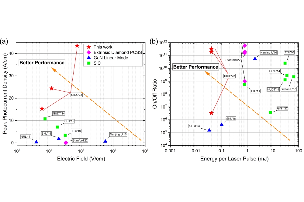
However, conventional PCSS, invented in 1970, have yet to reach necessary voltage/current levels at the voltage/current slew-rates required for power grid protection.This is down to three factors. First, they rely on traditional semiconductors which have low critical electric field (Ecritical) and thermal conductivity (κ). Second they create filaments to reach high currents, which is unpredictable and destructive. And third they use sub-bandgap laser light for triggering, which requires intentional impurity incorporation and limits the PCSS device size (and hence current).
Diamond’s physical properties make it an excellent PCSS semiconductor material for high voltage and high-power switching applications, with practically no limit on thermal resistance. As an ultrawide bandgap (UWBG) semiconductor, diamond has a bandgap of 5.47 eV. Intrinsic diamond also has high critical E-field.
The PCSS device developed by Bayram and his team embodies a buried, metallic p+ current channel for reaching high current densities and an impurity-free diamond (Ecritical ~ 10 MV/cm; κ ≥ 2,100 W/m·K) for voltage handling. This, say the researchers, eliminates the half-a-century-old tradeoff in PCSS between power handling and speed.
The team reports a record current density (i.e., 44 A/cm under low DC bias of 60 V) with no theoretical limits on the achievable current density. In addition, the PCSS devices exhibit large on/off ratios (>1011) and fast rise and fall times (~2 ns).