Polychromatic pixels
MicroLEDs with a tuneable wavelength provide an unparalleled foundation for superior displays.
BY MICHELLE CHEN FROM Q-PIXEL INC.
FROM COMMUNICATIONS to entertainment, displays play a critical role in the human-computer interface, dominating the way we interact with data and information. Accordingly, it is important to optimise the design and engineering of all forms of display. The best technology allows outstanding displays to be a major plus point for the marketing of new generations of computers, phones, tablets, TVs, and smart wearables. While consumers have different tastes, they are all united in a desire for brighter, longer lasting, more energy-efficient, higher resolution displays – delivered at a lower cost. But what exactly makes the ideal display? And what technologies will get us there?
The ideal display
Displays that draw the eye and engage the user are bright, colourful, and crisp. However, when engineering and implementing a display, there’s a need to think beyond just these metrics. As well as the aesthetic appeal, good displays have a number of consumer-centric features, including a long lifetime, great energy efficiency and a low cost. It is the combination of all these factors that determines the overall performance and value proposition of the device or appliance that houses the given display.
While the criteria for an excellent display appear to be straightforward, no single display technology is commercially available today that encompasses all the desired characteristics. The mainstays of current display technology, liquid crystals and organic LEDs, dominate market share due to their low cost. However, both are held back by fundamental physics constraints, which are reflected in their disadvantages: short device lifetimes, issues with image burn-in, limited display resolution, and high power consumption. The latter is a major weakness, given that typically more than half a smartphone’s power consumption comes from just its screen. In a wireless world, where battery life is paramount, is there an optimal technology for a bright yet energy-efficient screen?
From a physics perspective, microLEDs based on compound semiconductor materials have long been considered the holy grail of the display industry. They are highly sought after for display technology due to a combination of attributes: self-emissivity, high energy efficiency, durability, extensive lifetime, fast response time, and the potential to provide a high pixel density and a superior display resolution. However, today’s microLED technology faces labour-intensive, cost-prohibitive manufacturing challenges that impede widespread commercialisation.
One notable bottleneck to realising microLED displays is the complex assembly methods required to make pixels capable of covering the entire visible light range. The traditional approach for accomplishing this task is to consolidate individually grown red, green, and blue (RGB) sub-pixels into one pixel. As industry moves to smaller pixel sizes to produce higher-resolution displays, RGB sub-pixel assembly is increasingly difficult and expensive. Another challenge is that the circuits that access the three individual RGB sub-pixels occupy finite space, further constraining pixel density and display resolution.

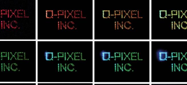
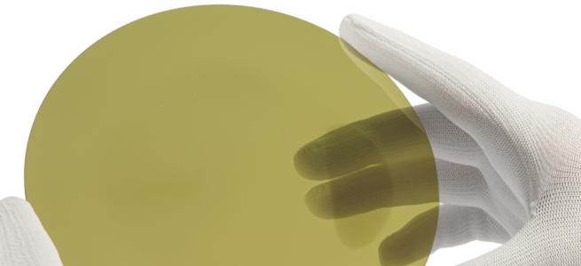
Figure 1. Wafer level demonstration of a polychromatic LED epi-wafer tuned across the entire visible spectrum.
Beyond century-old technology
The assembly of red, green, and blue sub-pixels for full-colour displays is deeply rooted in an obsolete aspect of LED technology: the monochromatic light approach. The first LED was fabricated almost a century ago. Since then, research in visible-light LEDs has emphasised materials capable of producing single-colour light of the highest quality and efficiency. While this has been indispensable for some applications, such as illumination lighting, the focus on monochromatic LEDs has inadvertently hindered the path to widespread adoption of microLED display manufacturing.
Due to the LED industry’s fixation on producing wafers that yield monochromatic light, there is a barrier towards full-colour displays that begins at the material level. Typically, efforts at manufacturing mini-and microLED displays begin with the production of separate epiwafers for the emitters of red, green, and blue wavelengths. To produce full-colour pixels, all three types of epiwafer are diced into chips, before miniature red, blue, and green emitters, or sub-pixels, are grouped to form one pixel on a driving backplane.
The positioning of the red, green and blue chips to form a full-colour pixel – a process known as mass transfer – demands precision accuracy and high yield. Unfortunately, current mass transfer technology is by far the most expensive and least reliable step of microLED display assembly, due to its low throughput, and the need for extensive testing and repair, especially as pixels become smaller. The result is that mass transfer of individual red, green, and blue sub-pixels is a major showstopper to the commercial viability of microLED displays. With 4K televisions having over 8 million pixels (or 24 million RGB sub-pixels), it is easy to see why microLED display products are yet to be an affordable or widespread offering within the mainstream consumer market.
A polychromatic paradigm shift
At Q-Pixel, a Los Angeles based start-up focusing on LED innovations, we are side stepping the monochromatic barrier while rapidly advancing microLED technology towards commercialisation. The secret to our success lies in an entirely different approach to both LED design and the traditional methods of microLED pixel assembly. Rather than relying on monochromatic red, green, and blue LEDs grown on separate wafers, we pursue the monolithic growth of tuneable-wavelength LEDs to realise the full visible spectrum.
Lying at the very core of our tuneable polychromatic microLEDs is the material: uniform, full-colour tunability LEDs, grown across a single compound semiconductor wafer and tuned using one current driving channel, without any use of sub-pixels, quantum dots, colour filters, polarisers, or mechanical stacking. When combined with innovative fabrication processes, our wafers yield single pixels capable of emitting light across the full spectrum of visible colour.
The approach that we take to realising full-colour tunability is one that has been explored using different techniques over the years. Our method involves producing a GaN-based active region designed for red, green, and blue emission, where colour is tuned through different applied voltages. Compared to different groups’ approaches, our main advantage lies in the production of monolithic LEDs using fully industry-compatible processes, which deliver full colour tunability using a single current driving channel, over a small voltage range compatible with conventional display drivers.
Our game-changing technologies, involving proprietary growth, process, and assembly methods, promises to overcome the major manufacturing obstacles currently faced by the entire display industry in implementing microLED-based displays. By replacing red, green and blue sub-pixels with a single colour-tuneable LED, we eliminate the bottleneck of sorting, binning, and picking-and-placing separate LED sub-pixels, and we replace mass transfer with simplified assembly processes. Reducing these costly, time-consuming steps significantly streamlines full-colour display assembly and lowers manufacturing overhead. In addition, the use of a single polychromatic LED in a pixel – rather than three sub-pixels, plus their corresponding circuitry – promises new opportunities for realising the ultra-high pixel densities needed for superior-resolution displays.

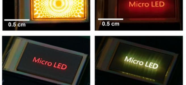
Figure 2. 10,000 pixels-per-inch passive microLED display with world’s smallest (1 µm diameter) full-colour pixels.
Revolutionising resolution
Ultra-high resolution is an urgent requirement for near-eye display applications, such as those used in virtual reality and augmented reality devices, as well as other head-mounted displays. The higher the display resolution, the less pronounced the undesirable ‘screen door effect’, a visual artefact that arises from visible gaps between large pixels or sub-pixels. Until recently, ultra-high resolution microLED displays, equating to more than 2,000 pixels per inch, had only been demonstrated in single colours, due to the constraints of assembling small red, green, and blue sub-pixels at ever increasing densities. Our tunable polychromatic LED technology has successfully surpassed this plateau, realising previously unattainable pixel densities in full-colour displays.
Last May we unveiled our full-colour microLED display with a record-breaking pixel density of 5,000 pixels per inch, far surpassing the previous world record of 2,000 pixels per inch. Six months later, we reported further progress, raising the bar to 10,000 pixels per inch for a full-colour microLED display. This more recent breakthrough broke two world records simultaneously: the highest resolution for a full-colour display; and the world’s smallest full-colour pixel to date, realised with an emitter with a 1 µm diameter.
At the beginning of this year we hit another important milestone, producing the world’s highest-resolution active-matrix colour display with our tuneable polychromatic technology. This astounding 6,800 pixel-per-inch display (around 1.1 cm by 0.55 cm, and around 3K by 1.5K pixels) is a landmark achievement, representing a first step towards widespread adoption of microLEDs by the display industry.
Bringing microLED displays to market ultimately comes down to a question of cost – in order to make microLEDs truly competitive in the display market, the cost of manufacturing needs to fall by over ten-fold from present rates – a target that can only be accomplished with a multi-faceted approach.
We have addressed this by developing scalable, cost-effective manufacturing technologies for microLED displays. Our emphasis is on assembly processes that minimise the number of defective pixels and maximise assembly speed for high-yield, high-throughput, large-area microLED displays. To remain competitive in a diverse market, we have devised assembly methods that are applicable to a wide range of display sizes and their respective applications, such as: televisions, tablets, personal computers, smartphones, automobiles, and wearable devices.

Figure 3. World’s highest resolution (6,800 pixels-per-inch) active-matrix microLED display.
MicroLED moment
Up until now, microLED technology has struggled to find a footing in the display and consumer electronics market. It has been impeded by the cost and inefficiency of the manufacturing process, a limitation so severe that it has made microLED technology impractical to compete with existing display technologies.
Meanwhile, existing display technology has stagnated, despite being a multi-billion-dollar market. Lack of new progress in displays is evidenced by major industry players and start-ups scrambling towards new technological solutions. The entire display industry is now on the cusp of a major paradigm shift, with microLED displays tipped to play a major role in eventually succeeding technologies based on organic LEDs and LCDs. It is not so much a question of if, but when the industry will adopt microLED technology. However, while the direction of travel is certain, there is still the ever-present question of which technological approach will be adopted in the process.
Our technological achievements provide early evidence that it is possible to produce cost-competitive, colourful, ultra-high resolution microLED displays. By moving beyond the traditional red, green, blue sub-pixel assembly and into the realm of the polychromatic pixel, we have effectively eliminated the most expensive step of microLED display manufacturing, without compromising quality. By delivering the world’s highest-resolution active display in colour, as well as demonstrating commercially viable microLED displays, we have proven that tuneable polychromatic LED pixel technology surpasses all current display technologies – even highly mature OLED technology – in making ultra-high-resolution displays.
Now the moment for microLED displays has arrived, and its future looks bright.