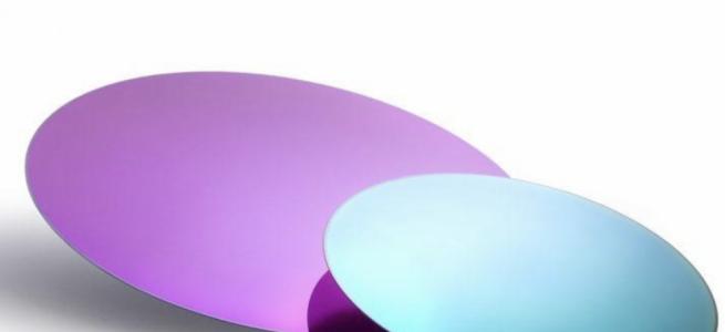
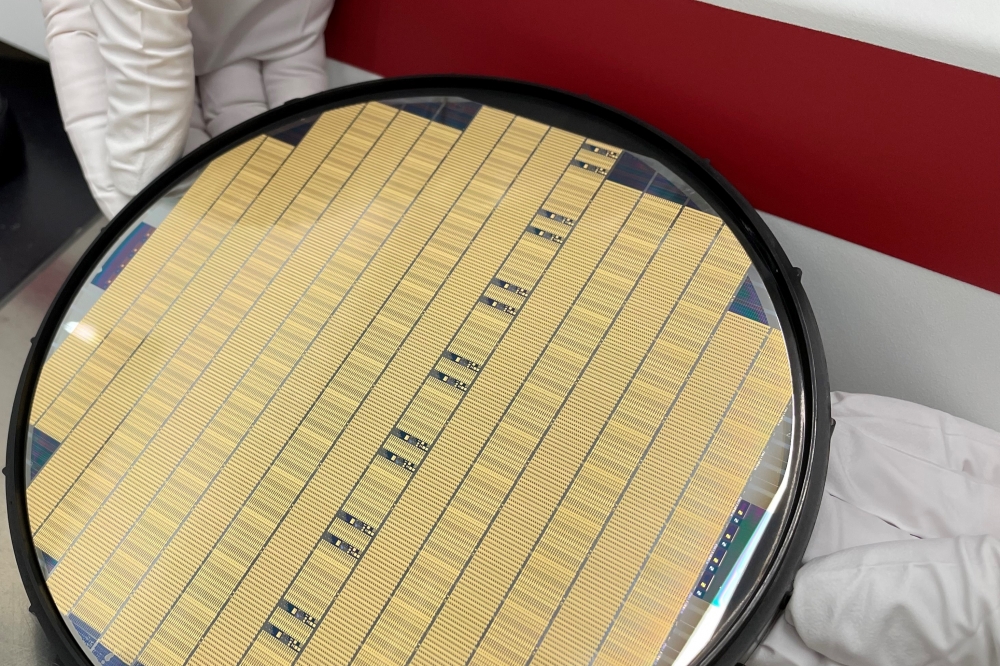
World’s first 6-inch InP scalable wafer fabs
Coherent paves the way for next generation of lasers for AI transceivers and 6G comms
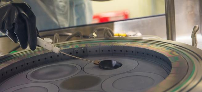
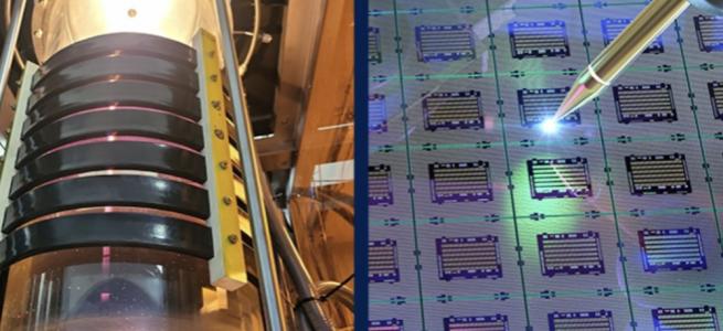
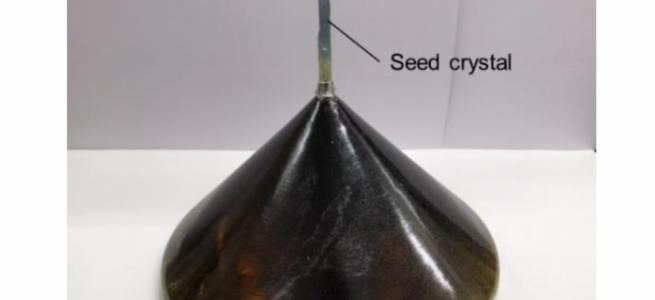
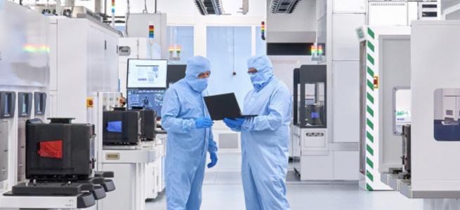
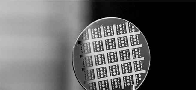
Coherent has established the world’s first capability for 6-inch InP wafer fabrication, in the company’s Sherman, Texas, and Järfälla, Sweden, wafer fabs.
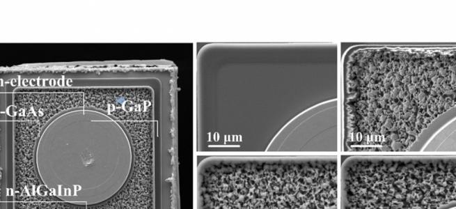
This milestone enables Coherent to increase production capacity and lower die costs for InP optoelectronic devices, widely used in applications such as coherent optical communications, datacom transceivers, AI interconnects, advanced sensing for consumer electronics and wearables, medical and automotive applications, and, in the future, in 6G wireless and satellite communications networks.
“We are very excited to announce our 6-inch InP wafer fabrication capability in both our Sherman and Järfälla fabs, which is a result of our continuous investment in innovation and technology development, and our years of investment and operating experience in high-volume VCSEL array manufacturing for mobile handsets,” said Giovanni Barbarossa, chief strategy officer and president, Materials Segment.
“Vertical integration at scale is a core strategy that we have been relying upon in several of our markets, and it has enabled our optoelectronics products to win in the marketplace by delivering world-class quality, performance, time-to-market, and cost advantage.”
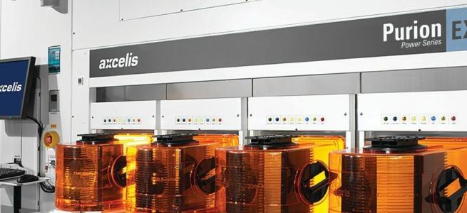
“Moving to 6-inch wafers will enable us to continue to deliver massive productivity improvements, including manufacturing 4x the number of devices per wafer, achieve a greater than 60 percent reduction in die cost, and allow us to transition our fabs to higher-capacity, more-efficient automated process tools,” said Beck Mason, executive VP, Telecommunications. “This capability will allow us to meet the growing demand for our InP products in several of our core markets, while enhancing our competitiveness and profitability.”