NCT grows 6-inch gallium oxide crystal
Vertical Bridgman technique paves way for larger high quality wafers
Novel Crystal Technology (NCT), a specialist in Ga2O3 technology, has successfully grown the first 6-inch Ga2O3 single crystal using the Vertical Bridgman (VB) technique. This achievement marks a significant step forward in NCT's efforts to deliver larger, high-quality semiconductor wafers for Ga2O3-based power devices.
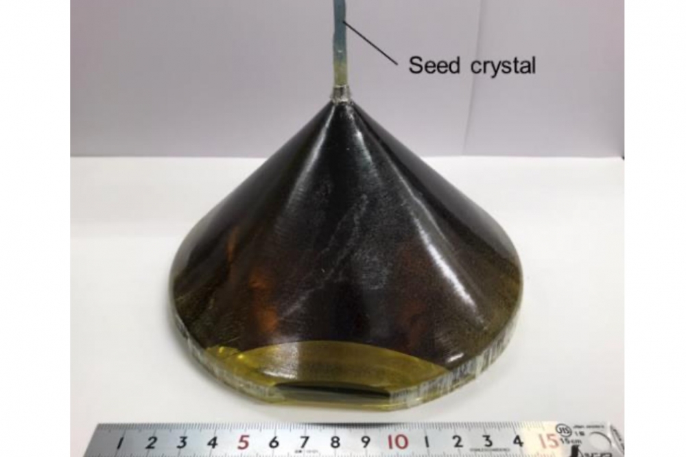
The development of the Vertical Bridgman growth technique (pictured above) for Ga2O3 single crystals was initiated by Shinshu University, successfully achieving growth of 2-inch and 4-inch crystals. NCT acquired and extended their techniques to enable larger diameter crystal development.
The VB technique offers several advantages over NCT's existing Edge-defined Film-fed Growth (EFG) method. By growing the crystal in a cylindrical shape, VB significantly reduces costs associated with substrate cutting. Additionally, it allows for production of substrates in various crystalline orientations, unrestricted by limitations imposed by crystal anisotropy.
Furthermore, the controlled thermal environment of VB growth leads to superior crystal quality with minimal defects, compared to EFG. Finally, dopant uniformity within the substrate is expected to improve, aligning with industry standards for other semiconductors like silicon.
NCT carried out a comparative evaluation between VB and EFG crystals with National Institute of Advanced Industrial Science and Technology (AIST) revealed a dramatic improvement in crystal quality. Synchrotron radiation X-ray topography analysis confirmed minimal defects in the VB-grown crystal, compared to the high density of defects observed in the EFG-grown crystal. This clearly demonstrates the superiority of the VB technique for producing high-quality Ga2O3 substrates.
Established in 2015, NCT manufactures 2-inch and 100 mm Ga2O3 substrates and epi-wafers for power devices. These are commercially available and used by universities, institutes, and power device companies worldwide.
NCT is actively developing larger substrates such as 6-inch. Beyond substrates, NCT has a vision for broader Ga2O3 device production. They are already offering samples of their first Ga2O3 Schottky Barrier Diode, with qualification tests expected to be completed in September 2024.
This research and development program was partially funded by the Adaptable and Seamless Technology Transfer Program through Target Driven R&D (A-STEP) of the Japan Science and Technology Agency (JST).