NIST finds way to centre quantum dots
Traceable microscopy could improve reliability of quantum information technologies, biological imaging, and more
Devices that capture the light from millions of quantum dots, including chip-scale lasers and optical amplifiers, have made the transition from lab to commercial products. But newer types of quantum-dot devices have been slower to come to market because they require extraordinarily accurate alignment between individual dots and the miniature optics that extract and guide the emitted radiation.
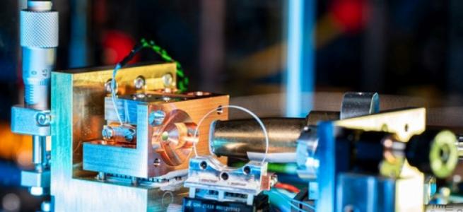
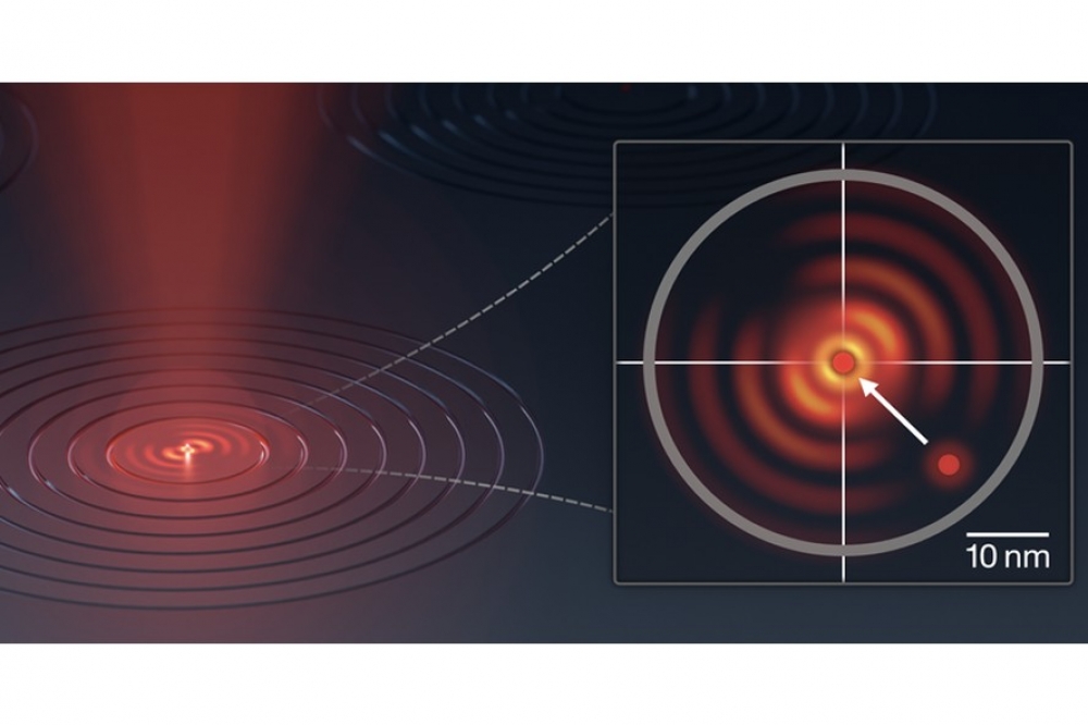
Researchers at the US National Institute of Standards and Technology (NIST) and their colleagues have now developed standards and calibrations for optical microscopes that allow quantum dots to be aligned with the centre of a photonic component to within an error of 10 to 20 nm. Such alignment is critical for chip-scale devices that employ the radiation emitted by quantum dots to store and transmit quantum information.
The NIST researchers achieved this level of accuracy across the entire image from an optical microscope, enabling them to correct the positions of many individual quantum dots.
A model developed by the researchers predicts that if microscopes are calibrated using the new standards, then the number of high-performance devices could increase by as much as a hundred-fold.
That new ability could enable quantum information technologies that are slowly emerging from research laboratories to be more reliably studied and efficiently developed into commercial products.
In developing their method, Craig Copeland, Samuel Stavis, and their collaborators, including colleagues from the Joint Quantum Institute (JQI), a research partnership between NIST and the University of Maryland, created standards and calibrations that were traceable to the International System of Units (SI) for optical microscopes used to guide the alignment of quantum dots.
“The seemingly simple idea of finding a quantum dot and placing a photonic component on it turns out to be a tricky measurement problem,” Copeland said.
In a typical measurement, errors begin to accumulate as researchers use an optical microscope to find the location of individual quantum dots, which reside at random locations on the surface of a semiconductor material. If researchers ignore the shrinkage of semiconductor materials at the ultracold temperatures at which quantum dots operate, the errors grow larger. Further complicating matters, these measurement errors are compounded by inaccuracies in the fabrication process that researchers use to make their calibration standards, which also affects the placement of the photonic components.
The NIST method, which the researchers described in an article 'Traceable localization enables accurate integration of quantum emitters and photonic structures with high yield' posted online in Optica Quantum on March 18, identifies and corrects such errors, which were previously overlooked.
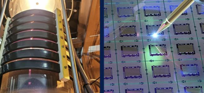
The NIST team created two types of traceable standards to calibrate optical microscopes—first at room temperature to analyse the fabrication process, and then at cryogenic temperatures to measure the location of quantum dots. Building on their previous work, the room-temperature standard consisted of an array of nanoscale holes spaced a set distance apart in a metal film.
The researchers then measured the actual positions of the holes with an atomic force microscope, ensuring that the positions were traceable to the SI. By comparing the apparent positions of the holes as viewed by the optical microscope with the actual positions, the researchers assessed errors from magnification calibration and image distortion of the optical microscope. The calibrated optical microscope could then be used to rapidly measure other standards that the researchers fabricated, enabling a statistical analysis of the accuracy and variability of the process.
“Good statistics are essential to every link in a traceability chain,” said NIST researcher Adam Pintar, a coauthor of the article.
Extending their method to low temperatures, the research team calibrated an ultracold optical microscope for imaging quantum dots. To perform this calibration, the team created a new microscopy standard—an array of pillars fabricated on a silicon wafer. The scientists worked with silicon because the shrinkage of the material at low temperatures has been accurately measured.
The researchers discovered several pitfalls in calibrating the magnification of cryogenic optical microscopes, which tend to have worse image distortion than microscopes operating at room temperature. These optical imperfections bend the images of straight lines into gnarled curves that the calibration effectively straightens out. If uncorrected, the image distortion causes large errors in determining the position of quantum dots and in aligning the dots within targets, waveguides, or other light-controlling devices.
“These errors have likely prevented researchers from fabricating devices that perform as predicted,” said NIST researcher Marcelo Davanco, a coauthor of the article.
The researchers developed a detailed model of the measurement and fabrication errors in integrating quantum dots with chip-scale photonic components. They studied how these errors limit the ability of quantum-dot devices to perform as designed, finding the potential for a hundred-fold improvement.
“A researcher might be happy if one out of a hundred devices works for their first experiment, but a manufacturer might need ninety-nine out of a hundred devices to work,” Stavis noted. “Our work is a leap ahead in this lab-to-fab transition.”
Beyond quantum-dot devices, traceable standards and calibrations under development at NIST may improve accuracy and reliability in other demanding applications of optical microscopy, such as imaging brain cells and mapping neural connections.