Rice team records 2D crystal synthesis in real time

Mini CVD system could help predict conditions for growing very large, single-layer MoS2 crystals
Materials scientists at Rice University in the US are shedding light on the intricate growth processes of 2D crystals, paving the way for controlled synthesis of these materials with unprecedented precision.
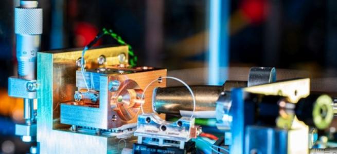
They have developed a custom-built miniaturised chemical vapour deposition (CVD) system capable of observing and recording the growth of 2D MoS2 crystals in real time. The work 'Towards Controlled Synthesis of 2D Crystals by CVD: Learning from the Real-time Crystal Morphology Evolutions' is published online in the journal Nano Letters.
They say that using advanced image processing and machine learning algorithms, they were able to watch real-time footage, that would help them predict the conditions needed to grow very large, single-layer MoS2 crystals.
Driven by their success with MoS2, the researchers believe their approach can be extended to other 2D materials and heterostructures, offering a powerful platform for designing and engineering next-generation 2D materials with tailored properties.
“For example, in electronics, being able to robustly synthesize 2D crystals like MoS2 at scale could lead to faster and more efficient devices,” said study co-author Jun Lou, professor and associate chair of the Department of Materials Science and Nanoengineering at Rice. “In sensors, it could lead to more sensitive and selective devices.”
“This research is an important step toward realising the full potential of 2D materials and paves the way for the development of innovative technologies that could revolutionise a wide range of industries,” said Ming Tang, associate professor of materials science and nanoengineering and study co-author.
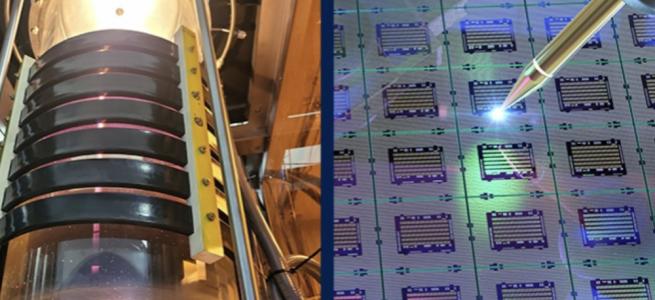
Pictured above: False-colour optical image of the MoS2 crystals grown at a high temperature and low flow rate, where the largest average crystal size is obtained among the tested growth conditions.