Realising avalanche in GaN-on-silicon diodes
Thanks to a low dislocation density in the epilayers, GaN-on-silicon diodes with a blocking capability above 800 V are capable of avalanche behaviour
A collaboration between engineers at the University of Lille and Siltronic is claiming to have broken new ground by producing the first GaN-on-silicon diodes with avalanche capability. The team’s vertical devices, offering avalanche capability, combine the high performance of a wide bandgap semiconductor with the low cost of large diameter silicon substrates.
Benefits of avalanche capability include providing a safety margin at the system level, and by operating safely at close to breakdown, an opportunity to use relatively small devices.
“Lateral GaN HEMTs cannot offer avalanche due to the peak electric field at the gate vicinity,” explains team spokesman Youssef Hamdaoui from the University of Lille. He adds that one consequence of this is that the safe operating voltage of the lateral devices is typically much lower than the hard breakdown voltage. “Such a voltage derating results in large gate-drain distances and therefore large device dimensions.”
Prior to this recent work of Hamdaoui and co-workers, GaN devices with avalanche capability had been limited to: native substrates, which are expensive; and sapphire substrates, which are held back by low thermal dissipation.
Hamdaoui believes that the team’s triumph will raise a few eyebrows within the wide bandgap power electronics community, because the high dislocation densities associated with GaN growth on silicon were thought to prevent avalanche capability.
Growth of the team’s epiwafers took place at Siltronic, using an industrial MOCVD reactor capable of accommodating 150 mm wafers.
“The quality of material was enhanced by a specific engineered buffer that helps to filter the dislocation density,” remarks Hamdaoui, who adds that the specific details of this approach will be published later this year.
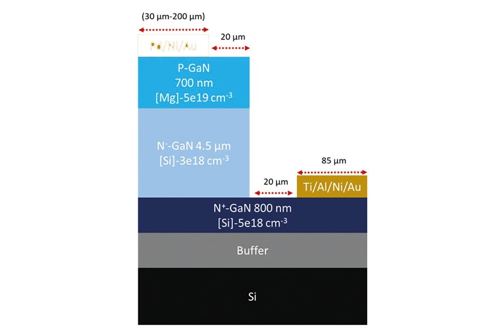
Fabrication of the diodes began by loading a 150 mm silicon substrate in an MOCVD reactor and depositing a proprietary buffer stack, followed by an 800 nm-thick n+ GaN layer, a 4.5 µm-thick n-type GaN drift layer, and a 700 nm-thick p-type GaN layer.
Plasma-enhanced CVD of a SiO2 layer that is patterned by reactive-ion etching created a hard mask for mesa etching, undertaken with an inductively coupled plasma process. The engineers etched deep into the epistructure, reaching the n+ GaN layer, and creating sidewalls with an angle of 75° that spread the electric field at the edge of the device over a distance that is larger than the drift region thickness. By taking this approach, it is possible to manage the electric field around the anode electrode.
To complete the fabrication of the diodes, Hamdaoui and co-workers added n-type and p-type contacts (see figure for more device details).
Measurements of the forward characteristics of diodes with a 30 µm anode diameter and a 70 µm top mesa diameter revealed a threshold voltage of 4.5 V and a differential on-state resistance below 0.35 mΩ cm2. According to the engineers, a lower threshold voltage can be realised by optimising the p-type ohmic contact.
Investigations of reverse characteristics revealed a blocking capability above 800 V, corresponding to an estimated critical peak electric field of 2.3 MV/cm.
Studying reverse characteristics of current density as a function of voltage at different temperatures enabled the team to determine that under a high reverse bias, carriers flow through a specific path with high energy, enabling the accumulation of additional charge carriers. This is said to lead to impact ionisation, which enables avalanche capability. The team also observed an increase in breakdown voltage with increasing temperature. This is claimed to be a strong indication of avalanche capability.
Hamdaoui and co-workers are planning to continue to optimise their vertical GaN-on silicon devices. The short-term goal is to produce 1200 V class diodes with avalanche breakdown capability. Looking further ahead, they are aiming to develop vertical transistors, such as trench MOSFETs, based on their optimised material system.
Reference
Y. Hamdaoui et al. Appl. Phys. Express 17 016503 (2024)
Pictured above: Avalanche capability is realised with pseudo-vertical GaN-on-silicon diodes