PCSELs produce green emission
By adjusting the dimensions of a photonic crystal, green emission is arbitrarily tuned over a 15nm range
A partnership between Nichia and Kyoto University is claiming to have produced the first photonic-crystal surface-emitting laser (PCSEL) that emits in the green part of the spectrum.
Spokesman for this team from Japan, Natsuo Taguchi, who holds positions at both Nichia and Kyoto University, says that green PCSELs have high potential, thanks to their tremendous beam quality. This class of laser produces single-mode operation in both the vertical and lateral direction, and combines a narrow divergence angle with a beam quality that is close to that of an ideal Gaussian beam.
Green-emitting PCSELs could replace solid-state lasers, according to Taguchi, winning deployment in applications that including imaging for displays and bioscience.
Another merit of the PCSEL is that it’s possible to engineer the emission wavelength with great precision through careful selection of the dimensions of the photonic structure.
“The lasing wavelength can be arbitrarily tuned,” says Taguchi, “which enables us to create arbitrary colours through colour mixing.” As well as providing a valuable attribute for display applications, this tunability allows emission to be tailored to the peak absorption efficiency of fluorescent dyes.
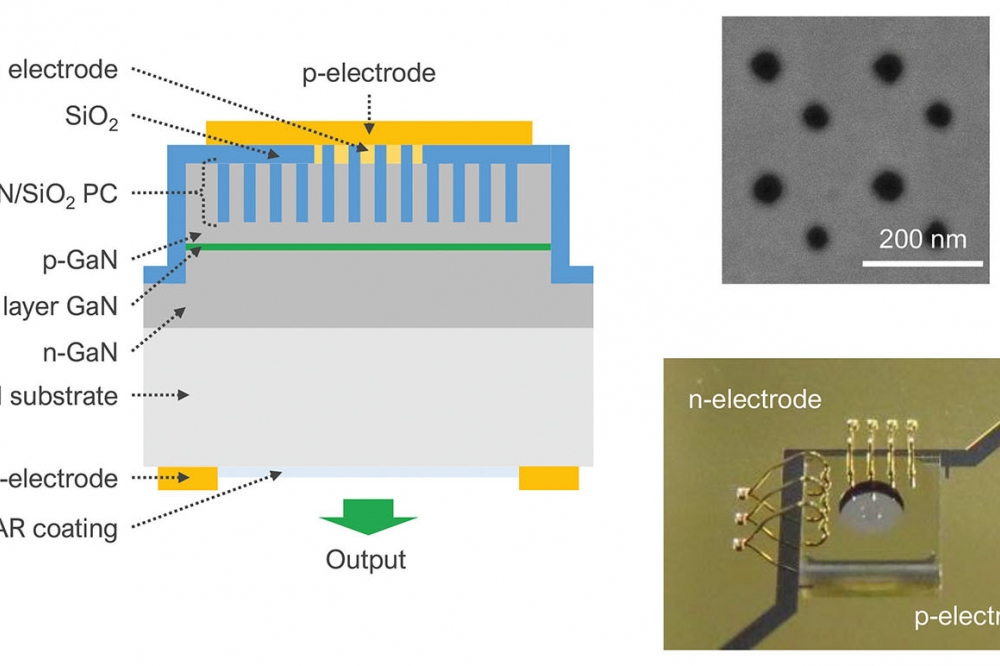
The green PCSEL pioneered by Taguchi and his colleagues features a double-lattice photonic crystal, incorporated to improve control over interference produced by the laser.
To form the photonic crystal structure, the engineers deposit a layer of indium tin oxide (ITO) above the GaN stack – a heterostructure consisting of an n-type layer, and active region and a p-type layer – and then use electron-beam lithography and reactive-ion etching to define device dimensions. By adopting this approach, it is possible to undertake optical characterisation of the epistructure via photoluminescence before finalising the details of the photonic crystal lattice.
Holes created by etching are filled with SiO2 using a plasma CVD process. This step protects the photonic crystal’s side walls from conducting particles, which threaten to cause current leakage and hamper stable operation of the PCSEL. Filling holes with SiO2 also increases the effective refractive index of the photonic crystal layer, leading to a shift in the distribution of the fundamental mode to this layer, and ultimately an enhanced coupling between the guided light and the photonic crystal.
Note, though, that there is also a downside associated with the addition of SiO2: a reduction in the refractive index contrast between the p-GaN layer and the photonic crystal. However, this can be offset by enlarging the fill factor of the photonic crystal.
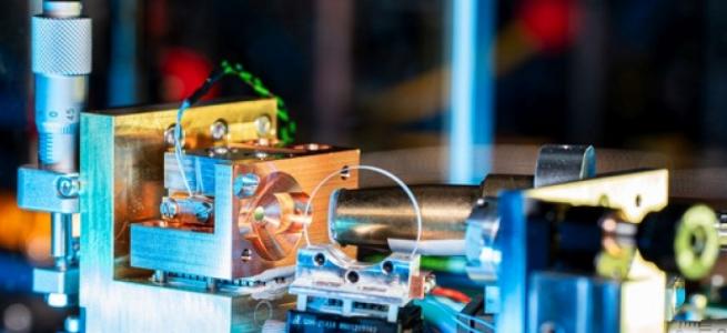
After filling the holes with SiO2, the team removed the ITO film, apart from a 300 mm-diameter central circular area that is used for an electrode, and then exposed the n-GaN layer, before adding electrodes and an anti-reflection coating (see figure above for the design of the PCSEL).
Driven with 500 ns pulses with a repetition frequency of 1 kHz, the team’s PCSEL produced a steep increase in power output at a current density of 3.89 kA cm-2, and delivered a maximum output of around 50 mW at a drive current of about 5 A. The corresponding wall-plug efficiency is around just 0.1 percent.
By adjusting the dimensions of the crystal lattice, the team demonstrated that it can arbitrarily tune the emission wavelength from 505.7 nm to 520.5 nm.
Taguchi says that one of the next goals is to increase the wall-plug efficiency of their PCSELs. This will be realised by optimising the design and the fabrication of the photonic crystals, to increase the intensity of in-plane coupling of the photonic crystal layer and vertical radiation. “Simultaneously, the epitaxial layer will be optimised to reduce the lasing threshold.”
Reference
N. Taguchi et al. Appl. Phys. Express 17 012002 (2024)