Advancing millimetre-wave GaN technology to 150 mm wafers
The vacuum tube electronics that serve the military for applications in
the W-band could soon be replaced by GaN MMICs, produced with a 140 nm
process using 150 mm wafers.
BY DAVE BROWN FROM BAE SYSTEMS
For a multitude of RF systems, a critical component is the GaN-based Monolithic Microwave Integrated Circuit (MMIC). Products incorporating this technology are deployed in wireless base stations, SATCOM terminals, and are a core enabler of 5G systems. In addition, due to a level of performance that’s not possible with silicon-based electronics, GaN MMICs feature in defence systems for radar, missile seekers, electronic warfare, and communications.
In all these applications GaN transistors make a welcome contribution, thanks to their capability to provide the best combination today for any semiconductor technology, judged in terms of high-frequency operation, low noise, high linearity, and high output power density.
RF GaN is now in a new era of maturity. RF systems employing this wide bandgap semiconductor are fielded across a broad range of domains and missions, with GaN MMICs with a high manufacturing readiness level present in a number of defence and commercial foundries throughout the world. Over the next decade this technology is sure to progress towards more advanced process nodes, featuring gate lengths below 150 nm. This scaling of dimensions will extend operating frequencies through the millimetre-wave spectrum towards 100 GHz while increasing instantaneous bandwidth. Simultaneously, there is a maturing of process capability, involving increased wafer diameters and line yields, that will drive up foundry capacity and reduce the cost per chip. It’s a direction of travel that will spur greater market penetration of GaN MMIC products.

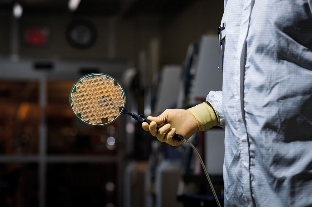
Figure 1. A completed 6-inch GaN-on-SiC wafer fabricated using BAE Systems’ 140 nm process.
At BAE Systems, a leading supplier of microelectronics, we are designing, developing and producing custom RF integrated circuits for a broad range of defence electronic systems. Our efforts are in demand, because MMIC-based products that meet the needs of the defence industry are rarely available from commercial sources, due to the complex nature of this technology, combined with unique and challenging performance requirements.
We produce our GaN-based MMICs at the BAE Systems’ Microelectronics Center (MEC). This is a Department of Defense (DoD) trusted foundry located in Nashua, NH, that’s dedicated to the manufacture of custom GaAs and GaN circuits.
Our MEC is a vertically integrated facility that has all the capabilities needed to develop and produce advanced microwave products. This 110,000 ft2 facility is home to a wafer foundry, MMIC and RF module design teams, on-wafer RF testing, wafer dicing, inspection, post processing, reliability qualification, a microwave module prototyping facility, and a production factory for microwave power amplifier modules utilising our GaN MMICs.
Established in 1984, our MEC has a long history of delivering GaAs and GaN-based microwave products for the DoD. One unique aspect of our foundry is the 150 mm wafer line, offering a higher product yield and a lower chip cost than the industry standard processes based on 100 mm diameter wafers. Our MEC’s 150 mm wafer processing line started running production GaAs processes in 2004, with the first 150 mm GaN MMICs reported ten years later.
The 150 mm GaN wafer processes developed at our MEC produce devices with a high yield, excellent performance and impressive reliability – the mean time-to-failure is more than 10 million hours at a channel temperature of 200 °C. In progress at the MEC is a multi-year modernisation project that will add wafer capacity, enabling us to keep pace with the growing demand within the DoD for advanced RF MMIC components.

Figure 2. Pulsed current-voltage (I-V) characteristics, including
current collapse and pulsed knee current, explored for devices with
different SiN passivation thickness. SiN thickness correlates strongly
with current collapse.
Miniaturising GaN
Back in 2018, BAE Systems signed a cooperative agreement with the Air Force Research Laboratory (AFRL) to transfer an advanced, high-performance 140 nm GaN process developed by AFRL’s research fabrication facility to our production-focused foundry. This new process, with a shorter gate length and superior transistor performance, augments our existing GaN capability and targets applications at millimetre-wave frequencies from 20 GHz to 50 GHz. This frequency domain helps us serve modern defence applications, which are now demanding higher operating frequencies and wider instantaneous bandwidth, often within small form factor payloads that have limited prime power and thermal management capability.
Often our state-of-the-art GaN production devices have an output power that is thermally-limited. To address this drawback, we have tailored our 140 nm GaN technology to offer improvements in gain and power-added efficiency at frequencies up to 50 GHz, while still providing sufficient output power density to meet mission requirements. Through this ‘lab to fab’ collaboration model, we have successfully transitioned our process and demonstrated state of the art performance, yield, and reliability on our 150 mm production line.

Figure 3. Ka-band load pull measurements at 35 GHz on devices with
different SiN thicknesses. Measured power, efficiency, and gain follow
expected trends, with thicker SiN reducing current collapse while also
increasing parasitic capacitance. A thickness of about 150 nm is optimal
for maximising power-added efficiency (PAE).
The epitaxial structure for our GaN MMICs is produced by loading SiC substrates in an MOCVD chamber and growing an iron-doped buffer, followed by a GaN channel, a 1 nm-thick AlN spacer, a 17 nm-thick Al0.28Ga0.72N layer and a 2 nm-thick GaN cap. We process our epiwafers into devices with a 140 nm gate length. They do not feature source-connected field plates, as this allows us to enhance device gain and reduce parasitic drain-to-source capacitance. Using a gate-source spacing of 0.5 µm and a gate-drain spacing of 2.0 µm, we trim the source resistance and realise a breakdown voltage in excess of 80 V.
To minimise source inductance and enable our microstrip MMICs to operate at high frequencies, we thin substrate thickness to 50 µm. To the best of our knowledge, this represents the first GaN MMIC process on 150 mm wafers that are thinned to that thickness.
During the development of our 150 mm MMIC process, we discovered that SiN passivation plays a crucial role in determining large-signal device performance. We investigated the impact of passivation thicknesses ranging from 50 nm to 250 nm on the maximum efficiency at Ka-band.
This work involved characterisation of 4 x 65 µm and 4 x 75 µm devices, using DC, small-signal, pulsed current-voltage, and Ka-band load-pull performance measurements.
Our devices exhibit a maximum drain current of more than 1.3 A/mm, with a peak transconductance in excess of 390 mS/mm. The DC characteristics are consistent across all passivation thickness variants. Our pulsed current-voltage characteristics on 140 nm devices with different SiN thicknesses are summarised in Figure 2. This data shows that there is a fall in current collapse as the thickness of passivation increases, a finding that is consistent with previous reports within the scientific literature.

Figure 4. Ka-band, CW, load pull power sweep measured on the optimised
device design at a drain voltage (VD) of 28 V, a drain current (ID) of
100 mA/ mm, and a frequency of 35 GHz. The device shows a peak
power-added efficiency (PAE) of 40 percent, with peak output power of
4.4 W/mm.
During load pull tests, we have observed a clear correlation between current collapse, the pulsed knee current and power performance (see Figure 3 for a summary of the load pull characteristics, such as output power, gain, power-added efficiency and drain efficiency, measured at 35 GHz for devices with different SiN passivation thicknesses). We have acquired our data at a peak power-added efficiency, using a drain voltage of 20 V and a drain current of 100 mA/mm, conditions that optimise efficiency. There is a clear trend in output power, which is boosted by thicker passivation. We attribute this to a greater reduction in current-collapse in the knee region of the current-voltage plane.
Plots of power-added efficiency follow a different trend, peaking for a SiN thickness of about 150 nm. The position of this peak is governed by both: the drain efficiency, which improves with thicker passivation, thanks to a reduction in current collapse; and a degradation in device gain with thicker passivation, due to additional parasitic capacitance. We have carried out a power sweep of this optimised device (see Figure 4). At nominal operating conditions of a drain-source voltage of 20 V, this optimised device has a cut-off frequency of 50 GHz and a maximum oscillation frequency of 145 GHz (see Figure 5).
Replacing tubes
In contrast to commercial uses, DoD RF applications target dominance of the full electromagnetic spectrum. This requirement drives a need for amplifiers that cover multiple octaves of instantaneous bandwidth with very high output power levels. Historically, this need has been met by travelling-wave tube amplifiers and other vacuum electronics. However, it is also possible to fulfil these requirements with GaN technology, as we demonstrated at the 2023 International Microwave Symposium in San Diego (Figure 6).
At that symposium we reported a 32-38 GHz MMIC. This three-stage, reactively matched power amplifier has a 5 mm by 6 mm footprint and 16.8 mm total transistor periphery. It is a design that uses a 1:2:4 drive ratio to provide sufficient drive to the output stage at baseplate temperatures of up to 125 °C, and features Lange couplers in a balanced configuration to realise efficient on-chip power combining and improve the voltage standing-wave ratio. There are some trade-offs in performance with our design to ensure unconditional stability at temperatures down to -50 °C. Even despite these trade-offs to performance, our MMIC deliver a 25 W output power at a power-added efficiency of more than 20 percent – this represents the highest measured output power from a single die at this frequency range.

Figure 5. Small signal RF measurements of the 140 nm technology,
measured on 4 x 75 µm unit cell devices. Under nominal operating
conditions, at a drain voltage of 20 V with a drain current (ID) 100
mA/mm, the devices achieve a cut-off frequency (fT) of 50 GHz and a
maximum oscillation frequency fmax of 145 GHz. The fT and fmax contour
plots show the impact of quiescent bias on the cut-off frequency.
We are now developing a new GaN technology. Based on a 90 nm HEMT process and leveraging advanced process features, this technology will enable amplifiers to deliver a higher performance while maintaining customer affordability. This process primarily targets power amplifier applications in the W-band, a frequency domain spanning 75 GHz to 110 GHz and encompassing a local minimum in the atmospheric absorption spectra. We expect this portion of the electromagnetic spectrum to be exploited by radar, missile seekers, synthetic-aperture radio imaging, E-band radio and 6G applications. In the near term, we expect that the proliferation of RF components in this frequency band will drive the need for the US DoD to access the best high-frequency GaN technology, to ensure that it maintains dominance over the electromagnetic spectrum. This need will be met by our 90 nm process, which we will qualify in the near future with 150 mm wafers.
Our goal is to continue to drive our GaN technology towards more advanced nodes that offer best-in-class defence electronics that meet the needs of the DoD and the warfighter. The electronic-warfare experience at BAE Systems spans more than 60 years, and over that time it has provided assistance in electronic support (rapid detection, missile warning), protection (RF/IR countermeasures, off- and on-board systems), and attack (threat analysis and response, RF/threat management). Our electronic-warfare systems operate on more than 80 percent of US fixed-wing military aircraft, including platforms such as F-15, B-2, F-22, and F-35.

Figure 6. Simulated (blue lines) and measured (black data points)
on-wafer power performance of the 32-38 GHz power amplifier MMIC
designed into BAE Systems’ 140 nm GaN technology
As part of our commitment to meet the needs of the DoD, we make our GaAs and GaN technologies accessible to the US Defense industry at large through our open foundry service, where we fabricate custom MMIC designs for our customers. We currently offer 100 nm and 70 nm GaAs pHEMT processes, in addition to our 180 nm and 140 nm GaN-on-SiC processes, all on a 150 mm wafer diameter.