A red-letter day for the microLED

Switching to the cubic form of GaN promises to address the low efficiency of the red microLED, a key ingredient in tomorrow’s head-mounted displays.
BY MARTIN LAMB FROM KUBOS SEMICONDUCTORS
Today, big technology players are driving an explosion of interest in augmented reality (AR) and virtual reality (VR) applications. It is a sector that will be worth many tens of billions of dollars by the end of this decade, and is already triggering frantic development activity within the supply chain. For providers of the key enabling hardware, components and materials, substantial investment has flowed in recent years, spurred on by the opportunity to make a significant contribution to cost-effective, head-mounted displays delivering a world-beating user experience.
A key enabling technology for all AR and VR headsets is the display. Candidate technologies that are being pursued include liquid-crystal-on-silicon (LCoS), organic LEDs (OLEDs), miniLEDs and microLEDs. Already a number of early, head-mounted display products have been launched, with the aim of establishing a foothold in the market.
It may appear that all of these display technologies are promising, since they offer some of the required functionality for AR/VR applications. But the harsh reality is that in many cases they are little more than stop-gaps, falling short of the target for a variety of reasons. High on this list of shortcomings are: a limited battery life; undesirable heating of the headset; and poor visibility of the display in bright conditions, a drawback that leads one to question the usefulness of this technology in genuine AR situations. And on top of these considerations, there is the issue of cost, as well as that of affordability for the consumer.

Figure 1. Efficiency versus wavelength for nitride and phosphide LEDs.
There is a relatively moderate fall in efficiency in nitride-based
devices as their size is reduced to 5 mm. For phosphide-based devices,
even reducing the lateral dimensions to 30 µm leads to a significant
reduction in efficiency.
It is widely acknowledged that if it can be made to work at a full commercial level, the microLED will offer the optimum combination of attributes for this application. By drawing on this miniature source of light, there is the potential to produce near-eye displays that combine affordability with a high efficiency and brightness. According to Yole Intelligence, microLED revenue driven by AR/VR applications will rocket towards the end of this decade, to potentially reach around $1 billion.
However, despite the many millions of dollars that have been invested in the development of the microLED and its associated technologies during the last few years, the commercial success of this emitter is incredibly limited. Today, the microLED is currently confined to a few high-end TV applications, where the resolution of the display can be catered for by simply shrinking current LED technology. When it comes to head-mounted displays, very few early product offerings employ microLEDs – OLEDs and LCoS are preferred, despite their limitations.
Given this state-of-affairs, it is obvious that despite significant progress, outstanding issues must be addressed surrounding microLED display technology. Towards the top of this to-do list is the industrial realisation of small-form LEDs with suitable efficiency at longer wavelengths, such as green, amber and red. That’s unlikely to be addressed with ease, as it appears that improvements in performance that come from squeezing conventional devices are dwindling. So, since a breakthrough is required, a radical approach is called for. However, there are constraints, as ideally the solution must drop into existing manufacturing lines, while delivering a better performance than today’s long-wavelength microLEDs.
A solution offering much promise is now in the early stages of commercialisation by our team, Kubos Semiconductors. Drawing on technology developed at the University of Cambridge, we initially focused on addressing the shortfall in LED efficiency in the green part of the spectrum, an issue commonly referred to as the ‘green gap’. However, recently we have started to expand our exploitation of cubic GaN, using this lesser-known form of GaN for the fabrication of longer-wavelength microLEDs. Read on to discover why cubic GaN holds the key to unlocking the AR/VR displays markets, and why conventional forms of LEDs are inherently compromised for these applications.

Figure 2. The relationship between quantum well thickness,
photoluminescence emission wavelength and photoluminescence intensity.
Source: University of Cambridge
Efficiency challenges
One of the primary pain points facing every would-be maker of microLED displays is the poor efficiency of small-form LEDs. While microLEDs are often defined as having lateral dimensions of less than 100 µm, for typical near-eye displays these dimensions have to shrink to the order of 5 µm and below. At such small dimensions efficiency takes a big hit and drags down critical system attributes in AR/VR headsets, notably those discussed previously. While it might be tempting to think that the brightness of low-efficiency displays can be offset by cranking up the drive current of the microLEDs, this compromises the battery life and generates more stray heat in the headset, which must be dispersed.
Typical high efficiency, large area LEDs are usually constructed from one of two material systems. At the heart of most blue and green emitters are diode structures fabricated from multiple layers of alloys of hexagonal crystalline indium gallium nitride (h-InGaN). Meanwhile, red devices are made from structures comprising multiple layers of alloys of cubic crystalline aluminium indium gallium phosphide (AlInGaP). For both classes of device, efficiency varies with wavelength (see Figure 1), creating an issue that industry continues to wrestle with.
The drivers behind these deleterious trends are well-documented. With the h-InGaN material system it is possible to produce large-scale, blue LEDs with very high efficiency, but this metric falls as the emission wavelength increases, with low values in the green and pitiful ones in the red.
Explaining this trend are the inherent internal electric fields, present in the quantum wells that form the active part of the device. These fields give rise to the Quantum Confined Stark Effect (QCSE), a phenomenon that pulls apart electrons and holes in the wells, thereby hampering the recombination process that is responsible for light emission. These electric fields are a consequence of both spontaneous polarisation, which results from the asymmetry of the hexagonal crystal lattice; and piezoelectric polarisation, driven by the strain in the structure that arises from the lattice mismatch between the InGaN alloy used in the active region, and the adjacent GaN layers and the substrate.
An additional drawback of the InGaN system is the unwanted consequences associated with increasing the indium content, which is needed to narrow the bandgap of the material and propel its emission to longer wavelengths. Sadly, rising indium content increases the mismatch between the active regions of the device and adjacent layers, resulting in an increase in strain, a stronger QCSE, and ultimately reduced radiative recombination in devices with a longer emission wavelength. Adding insult to injury, the stronger internal electric fields limit the width of the quantum wells that can be employed, and place further constraint on the tools that device designers need to access longer wavelengths.
With the AlInGaP system, it is possible to produce highly efficient, large-scale LEDs emitting in the red and amber. However, efforts to shorten the emission towards the green by adjusting alloy composition lead to a transition from a direct to an indirect bandgap for the quantum wells, thereby inhibiting carrier recombination and suppressing the device’s emission efficiency. Due to the limited bandgap of the phosphides, it is completely impossible to cover the blue end of the spectrum with this material system.
For the producers of AlInGaP, one consideration is the choice of substrate. Typically, they will use GaAs, or possibly GaP. The former is plentifully available at large diameter and reasonable cost, but it is possible that it could lead to concerns associated with the presence of arsenic in consumer applications. Meanwhile, the downside of GaP is that it is challenging to produce large diameter material, although it may be possible to overcome this by turning to a composite substrate. Nevertheless, despite these issues, and a lack of simplicity that comes from having to use two fundamentally different material systems to address the range of colours required for a display, the AlInGaP system does have potential for providing red devices, so long as they maintain their efficiency advantages over h-InGaN at the smaller scale.
And therein lies the problem. As is clear to see in Figure 1, the emission efficiency plummets when shrinking the lateral dimensions of LEDs made from these material systems to a few microns. This fall in efficiency stems from the increased ratio of sidewall surface area to active volume, a condition that causes recombination processes that occur at or near the sidewalls of the device to dominate its characteristics. If these processes result in the non-radiative recombination of carriers – and the evidence is that they do – the emission efficiency is greatly reduced in small form devices.
Managing these undesirable surface-related phenomena has been a major focus for the LED industry. Measures that have been taken include the application of coatings to passivate surfaces, and the use of thermal treatments to repair crystalline damage that’s inflicted by dry etching, which is used to form LED mesas.
In the h-InGaN system these treatments are reasonably effective: the material is reasonably hard and can be repaired, but the act of shrinking the device still results in a significant reduction in efficiency. Devices emitting in the blue and the green are probably adequate, particularly given the increased sensitivity of the human eye to green light, but in the red region where the underlying efficiency is already low for large LEDs, the reduction in scale makes the efficacy questionable in today’s small devices made in h-InGaN. For AlInGaP, the picture is even bleaker. In this material system there is a higher surface recombination velocity, which magnifies the surface recombination problem, and makes size reduction an even greater challenge. As a consequence of these efficiency-related issues, the production of red microLEDs based on either h-InGaN or AlInGaP remains a work-in-progress.
These problems have been well known for a long time. Efforts to tackle them date back more than a decade, and have been supported by millions of dollars of investment. But there’s yet to be a significant breakthrough – so perhaps it is time for a new approach.

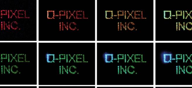
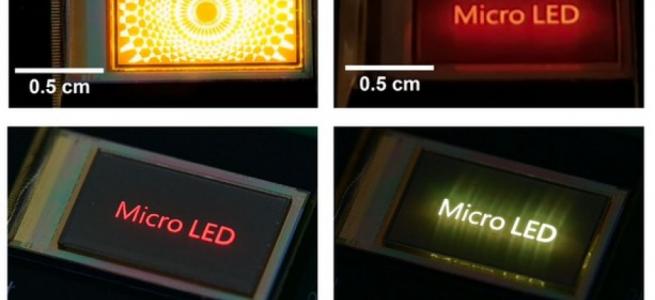
Figure 3. Kubos’ cubic InGaN microLEDs produced using MOCVD and demonstrating green, amber and red emission.
The case for cubic GaN
While many companies continue to throw money and resources at conventional material systems, there’s no sign of a breakthrough. What’s far more likely is progress on this front will continue to be slow, incremental and costly.
Given this unappealing prospect, there is much to like about the technology that we are pioneering. By taking a fundamentally different approach, we are opening the door to realising an efficiency performance in the longer-wavelength microLEDs that the industry craves, while ensuring that red, green and blue microLEDs can be produced with a single material system. In addition, our technology has the benefits of being fully scalable, and able to be simply ‘dropped into’ existing manufacturing lines. In short it is GaN, but not as the world knows it: it’s cubic GaN.
It has long been known that the group III nitrides, namely AlN, GaN and InN, and all their well-related alloys, tend to crystallise in a stable hexagonal structure. This is the structure of the LEDs that light our homes, our streets and our offices. However, the group III nitrides can also crystallise in a cubic structure. This alternative form, denoted c-GaN or c-InGaN for the ternary alloy, offers a number of potential benefits over the established structure.
One of the major benefits of c-GaN is that it is completely free from the internal electric fields that cause the QCSE and are to blame for the collapse in efficiency with increasing wavelength. The absence of internal electric fields, resulting from the higher symmetry of the cubic crystal structure, offers the possibility of using wider quantum wells to access longer wavelengths, an approach that’s precluded in h-InGaN devices. Another advantage is a reduction in screening at high drive currents, giving diminished blue shift compared to that observed in h-InGaN devices where a device might emit red light at low drive currents and yellow or green light as the current is increased.
Another advantage of c-GaN is its more favourable bandgap. For this form of GaN, the bandgap is 3.2 eV, compared to 3.4 eV for h-GaN. The reduction in bandgap means that the baseline emission from a device employing c-GaN will be at a longer wavelength, even before the addition of indium. Thanks to this, wells with a lower indium content can access a given wavelength when compared with h-InGaN devices, enabling improved crystal quality. It is also possible to turn to wider wells with this material system, thereby equipping device designers with an additional degree of freedom.
As well as these strengths, associated with the light-generation process, there are merits realised by superior carrier transport. In c-GaN it is possible to enjoy a higher hole mobility and a higher maximum hole concentration than it is in h-GaN. These are valued attributes, as the ability to realise highly conductive p-type layers is vital to successful LED operation at high current densities.
While c-GaN has many strengths over h-GaN, both materials have much in common. Consequently, it’s anticipated that the measures for mitigating the influence of a fall in device efficiency with scaling can be transferred from one form of GaN to another.
Given these very compelling arguments, on paper at least, c-GaN and its alloys are poised to revolutionise the microLED business, so long as the theoretical advantages can be delivered in practice.
State of play
We have made much progress with our technology. We have established and are now commercialising a reliable and scalable route for manufacturing single phase, cubic III-nitride epilayers. Our material is grown on a standard, vicinal (001) silicon substrate that’s coated with a thin epitaxial layer of 3c-SiC to provide a reasonable lattice match and a suitable cubic template. Growth involves industry-standard MOCVD equipment and precursors.
We have demonstrated growth on 150 mm diameter substrates and our potential to scale to larger diameters is clear. Additional advances include the fabrication of test diodes, using processes similar to those employed for h-InGaN.
One of the highlights of our progress to date is the confirmation that by switching from h-GaN to c-GaN it is possible to produce longer-wavelength emitters with considerably reduced indium content in the quantum wells. We have produced LEDs emitting at 540 nm with an indium content of 10 percent. In h-InGaN, such a device would typically require around 17 percent indium content at 450 nm.
Another potential benefit that we have verified is that wider wells can produce emission, thanks to the absence, or at least the substantial reduction, of the internal electric field within the device. We have produced emitters that have 10 nm-wide wells, which would lead to very little emission in h-InGaN (see Figure 2).
We have also demonstrated that this material system can be engineered to generate light across the whole visible spectrum, potentially opening the way for a monolithic solution.
In addition to these performance benefits, we have shown that it’s possible to process c-InGaN layers into test devices using existing manufacturing lines. This supports the thesis that the material might behave similarly to h-InGaN with respect to measures aimed at managing the impact of size reduction on LED efficiency. It also suggests that this material could be a drop-in replacement for h-InGaN.
While we still need to work on optimising the efficiency of the emission of our devices, we have already provided ample evidence that for any project aiming to produce adequate efficiency in the green, amber, and red, the cubic InGaN system is worthy of consideration.
Encouragingly, our work is already receiving recognition. Recently, we won support for a project aimed at making red microLEDs, with funding coming from Innovate UK’s Future Economy Investor Partnerships scheme. This investment will help us build on the exciting signs that cubic GaN can genuinely circumvent the physics that causes the bottleneck in the performance of longer-wavelength microLEDs, providing a near-term breakthrough for miniaturised red emitters that everyone has been looking for to unlock the AR/VR display market. Switching to the cubic form of GaN promises to address the low efficiency of the red microLED, a key ingredient in tomorrow’s head-mounted displays.