Ga₂O₃ ICs offer exceptional promise for extreme environments
Fabricating logic circuits and flash memory highlights the potential of Ga2O3 ICs for serving in extreme environments.
BY VISHAL KHANDELWAL, SARAVANAN YUVARAJA, XIAO TANG AND XIAOHANG LI FROM KAUST
Most computers have a relatively easy life. Whether in the form of a desktop, a laptop or a mobile device, they don’t tend to suffer from severe heat or cold, they don’t take much physical punishment, and thanks to the Earth’s magnetic fields, they are not bombarded by radiation.
But that’s not the case for all computers. Some have to endure extreme environments, including the likes of extreme cold, intense heat, electrical storms and high-energy radiation. For example, when computers are deployed in space missions, such as interplanetary space exploration, they are subjected to extreme temperatures and intense levels of radiation. High levels of radiation are also found in terrestrial nuclear reactors, while temperatures extremes are present at geothermal sites and in cryo electronics, a promising option for quantum computing.
At the heart of every computer are electronic ICs, which, when operating in extreme environments, have to function flawlessly under the likes of electrical storms, temperatures close to absolute zero and intense radiation. As these conditions threaten to damage and eventually degrade the IC, it is critical to develop electronics specifically designed to excel in these challenging environments.
For computers that operate in extreme environments, the two most important scenarios to consider are a high level of radiation and extreme temperatures. Each presents their own set of challenges and opportunities.

Table 1. Working conditions of electronics in extreme environments.
Let’s begin by considering radiation. This damages electronic systems through energetic particles and strong electromagnetic fields, creating issues that include resets, failures, signal glitches, noise, physical damage, and system shutdown. One of the drawbacks of most of today’s space electronics, which is based on silicon, is that it can only handle radiation up to 5 krad without damage. So, to operate in conditions where radiation is stronger, electronics are covered by heavy radiation-protecting shielding. However, even with this shielding, electronics degrades over time, reducing functionality and thus the lifetime of the space mission. For instance, the expected lifetime of satellites with silicon electronics is just 3 to 5 years, while the requirement for those in a geostationary orbit is much longer, typically 10 to 20 years. Due to this, solutions are needed to improve radiation tolerance in various digital and mixed-signal electronics, including ASICs and FPGAs, as well as complex heterogeneous integration microsystems.

Table 2. Physical properties of silicon, GaN, 4H-SiC, and Ga2O3 for applications in extreme environments.
In terms of temperature, standard silicon electronics is quite limited, with reliable operation possible between -40 °C to 150 °C. This is a major concern in a variety of applications. In oil and gas drilling, petrochemical applications and hypersonic vehicles, temperatures can reach up to 400 °C. In space, temperatures can be even higher – the surface of Venus is 460 °C – but in outer space is can be as low as −271 °C, so the electronics on board both space satellites and rovers has to operate over a very wide temperature range. To ensure optimal system performance, it is crucial that sensors, communications systems and control circuitry function effectively under these extreme temperatures.
Note that not all extreme conditions come from external factors; high power can stress microelectronics and their surroundings. Due to this, it is essential to develop new devices that are capable of managing high voltages, high currents and high powers, as well as advanced insulating materials and low-loss passive components. This approach is necessary to ensure the reliability and functionality of electronic systems operating in challenging environments.
Computing and material requirements
The use of computing chips in extreme environments is characterised by a greater variety of applications and heavy workloads. Specifically, in applications such as space exploration, the geothermal and petrochemical industries, as well as quantum computing, there is often the requirement for computers to be rugged, light, compact, and energy efficient. In addition, these computers must be capable of withstanding extreme conditions, such as low and high temperatures and strong radiation (see Table 1), ideally without having to draw on a heavy and bulky payload for temperature management and radiation shielding.

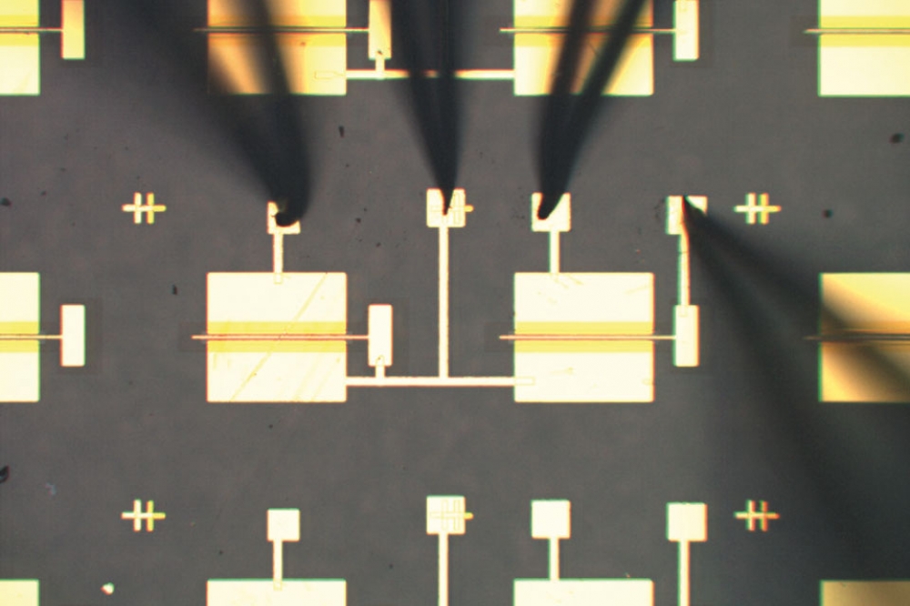
Figure 1. A Ga2O3 DCFL inverter (a) cross-sectional diagram. (b) An optical microscope image of the DCFL circuit.
For any electronic IC chip, the basic underlying technology is based on semiconductor materials capable of offering insulating and conducting properties, when subjected to an external electrical or optical ‘bias’. To build robust computing chips, ideally these materials can endure extreme environments. That means that as well as resisting melting, these materials are capable of withstanding potential failures caused by thermal or mechanical stress. In addition, they need to remain stable, avoiding degradation due to changes in their structure caused by heat, or surface damage resulting from the likes of diffusion, oxidation, vaporisation or ablation.
A number of elemental and compound semiconductor materials have been explored over the years, with efforts motivated by understanding their properties and determining their capability for producing various devices. Amongst them, silicon serves as the foundational source for all electronic innovations that exist in our daily lives. It is abundant and scalable, with a high mobility for electrons and holes, but due its narrow bandgap, its usage is constrained in harsh environmental conditions.
Two materials with a wider bandgap, GaN and SiC, provide a better performance, in terms of high temperature capability and radiation tolerance. However, both offer limited performance at low temperatures, with carriers in both bulk materials freezing out below 40K. (Note, though, that GaN transistors based on a polarisation-induced carrier gas are not sensitive to low temperature.) Additionally, GaN and SiC lack native oxides, potentially resulting in less stable IC operation in extreme environments. For instance, a single event burnout due to heavy ion damage is a big issue for SiC MOSFETs.

Figure 2. Ga2O3 dual-stage inverter circuits. (a) pseudo-R, (b)
pseudo-E, and (c) pseudo-D schematics. Fabricated devices with
transconductance ratio, KR, of 1. (d) pseudo-R. (e) pseudo-E. (f)
pseudo-D. Fabricated devices with a KR of 28.8. (g) pseudo-R. (h)
pseudo-E. (i) pseudo-D.
A far more attractive candidate may be Ga2O3. As well as being blessed with a larger bandgap than GaN and SiC, it offers well-balanced properties, and there are no significant drawbacks that might hinder its performance (see Table 2, which highlights the physical properties of silicon, GaN, 4H-SiC, and Ga2O3 for applications in extreme environments).
Ga2O3 is a great allrounder, offering superior properties in all extreme environmental conditions, including low and high temperatures and high levels of radiation, while maintaining a decent mobility. Another important attribute of Ga2O3 is that native bulk substrates can be produced at a lower cost than GaN and SiC substrates, crucial for low cost and scalability of ICs, thanks to the opportunity to use low-cost melt-grown techniques. Further improvement of heteroepitaxial Ga2O3 could further lower the cost significantly.
Blessed with an ultra-wide bandgap and extensive electron doping capabilities, Ga2O3 provides a promising solution for handling high powers – high-voltage and large-current electronics, as well as extreme temperature applications. During the last decade or so, Ga2O3-based transistors and Schottky diodes have been extensively studied, yielding impressive results that include a voltage handling capacity of around 8 kV and operational temperatures of up to 500 °C.
However, to operate in extreme environmental conditions, there is a need for electronic systems, which process and store information, to incorporate vital electronic components – specifically, logic circuits and flash memory built on Ga2O3.
Our team from King Abdullah University of Science and Technology (KAUST) is embarking on this challenge, and has already taken strides towards developing an advanced computing and memory chip that operates reliably in extreme temperatures. Breaking new ground, we have demonstrated the functionality of logic and memory components using heteroepitaxial β-Ga2O3, grown on a sapphire substrate. This triumph takes us closer to realising highly dependable, efficient, and compact computing systems designed to withstand extreme conditions.

Figure 3. (a) Scanning electron microscopy and (b) diagram of 3D-stacked
Ga2O3/NiO heterojunction ambipolar transistors. Here, Ga2O3 and NiO are
the n- and p-channels respectively. (c) Cross-sectional transmission
electron microscopy image of the gate region with zoom-in (d) bottom and
(e) top areas of a dome-shaped fin.
Initial investigations
Our research has focused on Ga2O3 logic inverter circuits based direct coupled FET logic (DCFL), pseudo-CMOS, and Ga2O3/NiO ambipolar CMOS ICs. We have also looked at Ga2O3 flash memory, designed with a floating gate configuration. Both our Ga2O3 logic circuits and our flash memory are realised on heteroepitaxial grown β-Ga2O3 on sapphire and silicon substrates.
The Ga2O3 DCFL inverter is realised through monolithic integration of top-gated normally-on (depletion-mode) and normally-off (enhancement-mode) Ga2O3 transistors. These devices, formed on sapphire substrates, work as a load and driver respectively. To realise normally-off operation, we employ a recess etched gate technique (see Figure 1(a) and (b) for a cross-sectional diagram and an optical microscopy image of Ga2O3 DCFL inverter circuits). This DCFL logic inverter shows successful operation, with a voltage gain of around 2.5 V.
Measurements show that our DCFL inverters, operating as single-stage inverters, exhibit elevated power dissipation. This arises from incomplete turn-off of the load thin-film transistor (TFT), when the driver TFT is active.

Figure 4. Floating gate Ga2O3 flash memory (a) cross-section schematic and (b) top microscope image.
One way to address this incomplete turn-off is to introduce pseudo-CMOS topologies – they minimise power loss by providing a more effective turn-off of both the load TFT during pull-down and of the driver TFT during pull-up. We fabricate these Ga2O3 pseudo-CMOS inverters in three configurations: pseudo-R, pseudo-E, and pseudo-D. The circuits use two different transconductance ratios, either 1 or 28.8 (see Figure 2). Note that the optimised pseudo-CMOS circuit exhibits the least peak power consumption, just 0.2 nW, and the maximum gain of 8 at a positive supply voltage, VDD, of 3 V.
To obtain a CMOS configuration, we have explored the seamless integration of Ga2O3 NMOS with p-type semiconductor-based PMOS. Using p-NiO, we fabricated the first Ga2O3-based ambipolar CMOS logic circuits with NiO and Ga2O3 as a p- and n-channels (see Figure 3). Notably, both the n- and p-channels offer excellent stability at temperatures of up to 300 °C.
Notably the Ga2O3/NiO ambipolar transistors comprise advanced gate-all-around and vertical-stacking architectures, showing that Ga2O3 ICs could benefit from processing technologies being established in latest silicon fabs.
Every electronic circuit requires a logic circuit to process the data, as well as memory to store it.
After realising our Ga2O3 logic circuit, we fabricated a heteroepitaxial Ga2O3 non-volatile flash memory using a conventional floating gate configuration. This involves using TiN for the floating gate, and Al2O3 for tunnelling and blocking oxides (see Figure 4(a) for cross-sectional schematics, and Figure 4(b) for the optical image of the fabricated device).
Our results are encouraging. The flash memory offers a large memory window of more than 4 V, and data retention is in excess of 5000 s. The programming operation of the memory provides a positive threshold voltage of 0.3 V, creating a new pathway for producing normally-off transistors for low static, low-loss electronic circuits.

Figure 5. Future vision: 3D heterogeneous integration of various
devices. Stacking involves combining various components made from
different semiconductor materials, with the goal of creating a highly
robust 3D heterogeneously integrated system for harsh environment
applications.
While Ga2O3 has great potential on its own, there is also the possibility for 3D integration with other material systems. It is possible for Ga2O3 logic ICs to be vertically stacked with SiC MOSFETs, Ga2O3 memories, GaN RF components and optoelectronic devices (see Figure 5). This shows that depending on application and environmental conditions, Ga2O3 may be used on its own to produce ICs, or combined with other material systems.
https://www.youtube.com/watch?v=YiouYISwBno&list=PLmUthPgVjKqNiYaIOdOprTz5YUl-7PhQw&index=6
https://www.youtube.com/watch?v=CmhSdKlLgfI&list=PLmUthPgVjKqNiYaIOdOprTz5YUl-7PhQw&index=5
https://www.youtube.com/watch?v=KuIgEB5i2YQ&list=PLmUthPgVjKqNiYaIOdOprTz5YUl-7PhQw&index=4