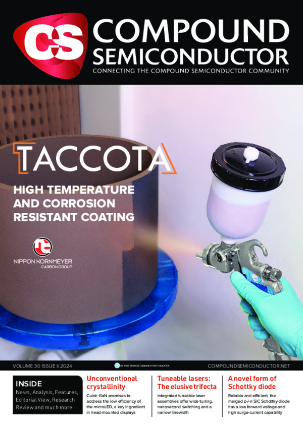
Coating at its best
Spraying graphite parts with tantalum carbide cuts the cost of producing SiC crystals and epilayers.
BY CHRISTIAN REIMANN, MATTHIAS TREMPA, KEVIN SCHUCK AND MICHAEL LANG FROM FRAUNHOFER IISB, AND TORSTEN KORNMEYER AND DIRK MUETZENICH FROM THE NIPPON KORNMEYER CARBON GROUP
The semiconductor industry is booming, with one prime example the field of SiC power electronics. Here many high-volume fabs are either under construction or expansion, to support an increase in the production of SiC devices, which are being deployed in electric vehicles.
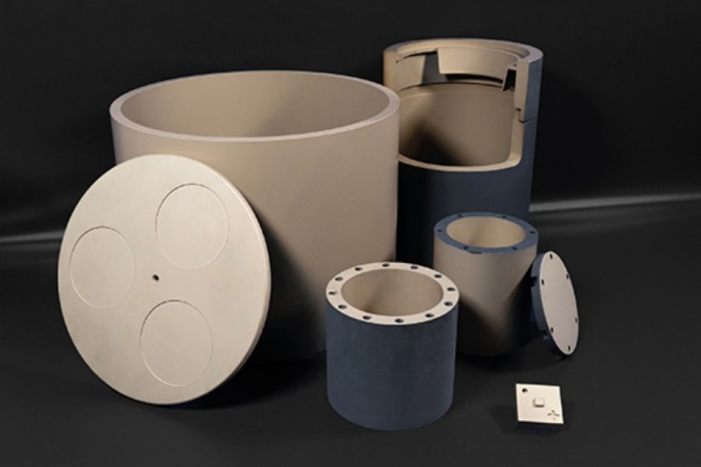
While every boom offers a great opportunity to increase profits, it also brings its own unique challenges. Crucial to ramping global SiC chip production is the manufacture of high-quality SiC crystals, wafers and epitaxial layers. In this context, it is crucial to consider the role of semiconductor-grade graphite materials, which are used in the equipment that enables the growth of SiC crystals and the deposition of SiC epitaxial layers. Graphite, which is valued for its thermal insulation capabilities and inertness, is the preferred material for crucibles and susceptors in crystal-growing systems, and for planetary discs and satellites in epitaxial systems.

Figure 1. The TaC process technology developed at Fraunhofer IISB allows
adjustment of desired coating properties, such as thickness, shown here
in the range 35 µm to 110 µm.
Killer degradation…
The production of SiC crystals involves harsh process conditions. The total corrosion of a graphite crucible may occur after just a few processes, due to temperatures of over 2000 °C and extremely corrosive gas species that contain silicon. For instance, the production of SiC epitaxial layers involves: process temperatures that peak at 1600 °C; the combination of silane and propane, which are responsible for the growth of the SiC layer; and hydrogen and in some cases hydrochloric acid. The latter two can be used as carrier gases, or for very corrosive etching.
As well as simply eating up the graphite components, the harsh process conditions alter the emissivity and morphology of the component surfaces. This is a significant issue, severely impairing the reproducibility of the production processes and in turn having an impact on the resulting process stability – and thus the material quality of the SiC crystals and epitaxial layers. Another major drawback is that the harsh conditions can cause free carbon and carbon particles to be released from the corroded graphite parts, threatening the production of high-quality SiC semiconductor material.
Due to these considerable concerns, process engineers tend to only use these heavily stressed components a few times, and sometimes just once. It is a constraint that causes consumable material graphite to contribute significantly to the manufacturing costs of SiC crystals and epitaxial layers.
…and graphite shortages
It’s of little surprise that graphite is in great demand in many sectors, due to its desirable physical and mechanical properties and its capability to form a wide range of geometries. Unfortunately, today’s graphite industry cannot keep pace with the strong expansion plans of the global SiC industry, and competition between end users for the best possible supply of graphite is already underway.
Fortunately, there’s a game-changing solution that kills two birds with one stone. It’s the introduction of protective layers, which tackle both the degradation of graphite parts and the graphite delivery shortage. It’s a most welcome introduction, given the drastic increase of lead times for graphite components, driven by the booming semiconductor sector.
Today, protective coatings based on tantalum carbide (TaC) are already in use. The merits of this material include a melting temperature of over 3800 °C and a very good chemical resistance to reactive gases. Up until now, the approach to producing state-of-the-art TaC protective coatings is to use Chemical Vapour Deposition (CVD) to deposit this material on graphite components, a process that produces semiconductor-clean and gas-tight layers with a thickness of typically up to 35 mm. However, there are disadvantages of this technology, with the main drawbacks including high manufacturing costs, and once again, long delivery times. In addition, there are material issues, with cracks appearing through 100 percent dense crystalline TaC layers during repeated heating and cooling of the components. These cracks expose the underlying graphite, which strongly degrades over time and has to be replaced.

Figure 2. Scratch test results of Tacotta spray coating with variable
thicknesses versus CVD TaC coatings performed after DIN50324 /ASTM G99
and G133. These results reveal an enhanced wear resistance due to
increased coating thickness.
The spray solution
Motivated by addressing all these shortcomings, those of us at Fraunhofer IISB started to develop a disruptive coating technology more than five years ago, with the aim of compensating for the disadvantages of the state-of-the-art approach. We began with very simple laboratory-scale tests, involving the coating and evaluation of graphite shards.
Over the years, our TaC coating technology has grown out of its children’s shoes. Helping on this front has been the feedback from potential end users – it has been key to the further development of our technology. Today, our patented approach combines a water-based spray coating with subsequent temperature treatment. One great asset of our technology is that it is incredibly flexible when it comes to coating components of different sizes and geometries. Unlike CVD deposition of TaC, partial coating and component refurbishment is also possible. What’s more, our technology is environmentally friendly, easy to industrialise, and free from conflicting materials.
We have evaluated the properties of our TaC coating. It is resistant to temperatures of more than 2500 °C and corrosive gases. The thickness of the coating is variably adjustable in the range of 20 µm to 200 µm (see Figure 1), ensuring protection impact for extremely lengthy process times and a high number of cycles. Another benefit of our technology is that it produces TaC coatings with tremendous mechanical stability, thanks to interlocking with the underlying porous graphite. We have demonstrated this attribute with so called scratching-tests (see Figure 2).
Following two years of pre-development, we shared the potential of this newly developed technology with a number of investors. Our technology impressed the Nippon Kornmeyer Carbon Group (NKCG), a joint-venture between the German-based Kornmeyer Group and Nippon Carbon Japan. They have licensed our technology from Fraunhofer IISB and produced TaC-coated graphite parts for their customers. Our collaboration, which started in 2021, immediately bore fruit. Already, the reusability of our TaC coating for the the production of SiC crystals has been successfully demonstrated several times. In addition to this valued reusability for SiC epitaxy, we have shown that there is no contamination from the TaC layer, and that the processed SiC wafers are free from any surface contamination (see Figure 3 and the text box “Proven coatings”).

Figure 3. SiC wafer carrier before (right) and after (left) several standard SiC epilayer processing runs.
We have even demonstrated that the tantalum contamination that occurs during epitaxy on SiC wafers with virgin TaC-coated graphite components is reduced by 75 percent in the first processes, compared with state-of-the-art CVD coatings. Thanks to this, our technology enables longer production campaigns with one graphite setup.
The uptake of the TaC coating technology, which we refer to as Taccota, has increased following its proven success in PVT and the epitaxial SiC crystal growth process. The management of NKCG is investing in a significant increase in production capacity along the entire value chain, from CIP feedstock to the TaC-coated finished parts, and it is also funding the introduction of an industry-leading quality control and management system. This investment is enabling NKCG to address the demand of graphite in this massive market, and fulfil its long-term strategic growth plan, together with its cooperation partner Fraunhofer IISB.