Finwave unveils latest GaN-on-Si tech
RF transistors, 3D Gan FinFETs and RF switches to feature at MWC Barcelona
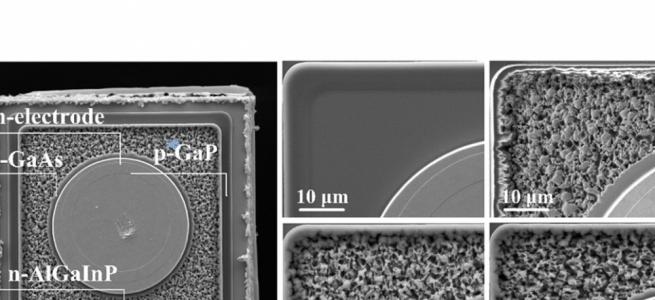
At MWC Barcelona, Finwave Semiconductor will unveil the newest performance benchmarks with its GaN-on-Si technology and high-power switches for infrastructure and handset applications.
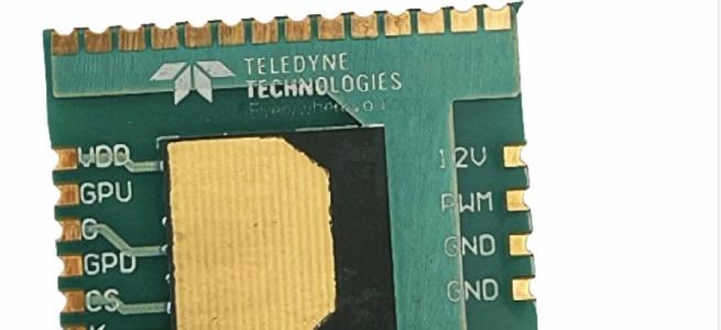
The company's enhancement-mode 200mm GaN-on-Si RF transistors, for example, have less than 1 ohm-mm on-resistance, low-knee voltage, > 700 mS/mm transconductance and negligible current collapse with power-added-efficiency (PAE) as high as 60 percent for operating frequency ranging from 8GHz to 26GHz.
The technology is capable of operating at Vdd of 5V or lower, demonstrating its potential for efficient power amplifiers for 6G FR3 frequency band (7-24GHz) and FR2 mmWave band infrastructure, CPEs and handset applications, according to the company.
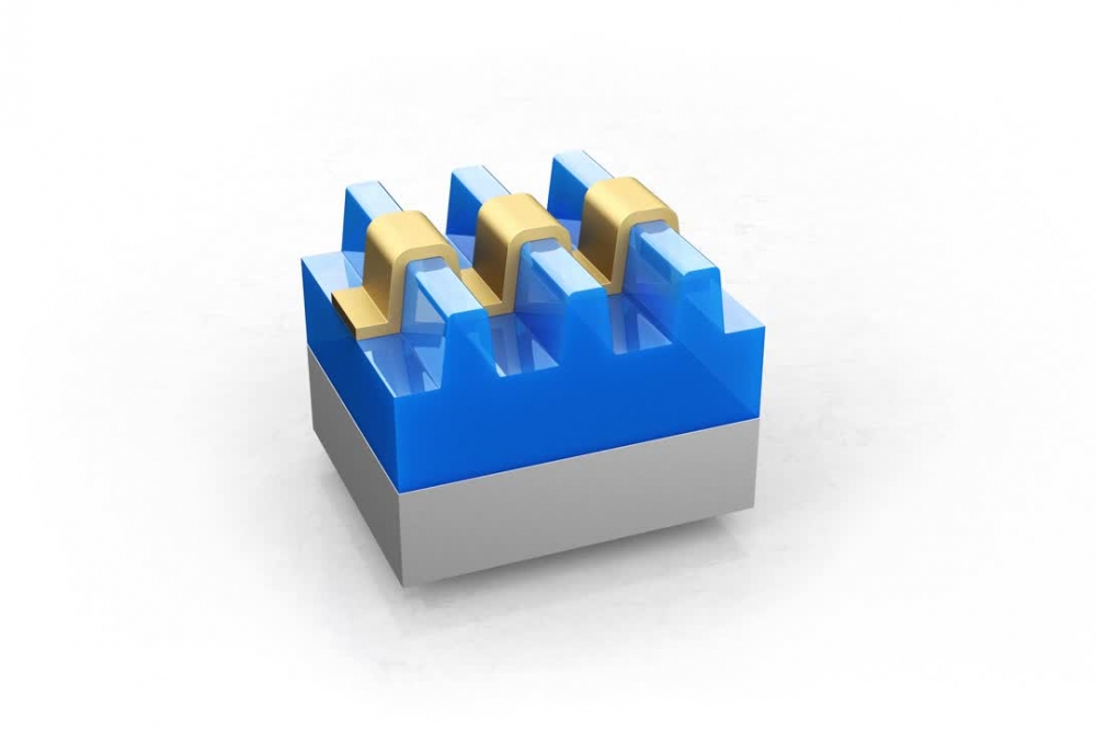
Finwave will also show 3DGaN FinFET technology demonstrating its linearity improvement capability. Due to its three-dimensional gate geometry, the 3DGaN FinFET reduces transistor leakage current, current collapse and knee voltage while improving PAE and linearity over 10dB compared to conventional GaN transistors.
With higher linearity, better PAE and reduced memory effect, 3DGaN FinFET technology is attractive for applications such as massive MIMO with large arrays.
Finwave will also unveil its first family of high-power RF switch products. The RF switch products feature 100ns fast switching and settling time, broadband operations up to 12GHz and high-power handling up to 40W. The combination of broadband operation, fast switching and high-power handling sets it apart from current offerings.
“Finwave is on the cusp of bringing the true potential of GaN to some of today’s most important enabling markets,” said Finwave Semiconductor CEO Pierre-Yves Lesaicherre. “Our technology has already demonstrated its ability to deliver extremely high performance in higher frequency applications, and the implications of that are very exciting – for both infrastructure and handsets. Additionally, we are making strong progress in moving our patented GaN-on-Si technology from the MIT lab to high-volume production.”