Nanowires for UVC emission
AlN nanowires with short-period superlattices based on AlN and GaN are
trailblazing a path to a new class of UVC-emitting devices.
BY
RÉMY VERMEERSCH AND CORENTIN GUÉRIN, BOTH AFFILATED TO CNRS-GRENOBLE AND
CEA-GRENOBLE; GWÉNOLÉ JACOPIN AND JULIEN PERNOT FROM CNRS-GRENOBLE; AND
BRUNO DAUDIN FROM CEA-GRENOBLE
IT IS WELL KNOWN that exposure to mercury is not good for our health. It can cause a number of symptoms, including tremors, insomnia, memory loss, neuromuscular effects, headaches and cognitive and motor dysfunction. Due to this, the current implementation of the Minamata convention, signed in 2017 under the auspices of the United Nations, is progressively banning the use of mercury-containing devices for environmental and sanitary reasons.
The phasing out of mercury has major implications for UV lighting. For emission in this spectral range, mercury lamps are the incumbent source, widely used for disinfection. As they will have to be replaced in the short term, the research and development of new UV-emitting devices is on the rise. Hopefully this will address the increasing need for versatile, efficient sources in the UVC range that spans 200 nm to 280 nm.
Optical sources that emit in this spectral domain can serve a variety of applications. That includes disinfection, as UVC light damages DNA (or RNA) chains, thereby preventing the reproduction of viruses and bacteria. However, while highly beneficial for disinfection, the sensitivity of DNA to UVC sources within this wavelength range is also problematic – it may severely hurt human skin, have long-term effects and cause melanoma. These downsides complicate the practical use of 265 nm UVC sources for the growing market of domestic disinfection applications, such as putting LEDs in a refrigerator, using them for tap water sanitisation and providing air purification.
Fortunately, humanity can enjoy the benefits of UVC sources while avoiding their pitfalls. What’s needed is to decrease the wavelength within the UVC to the 220-230 nm range. At such short wavelengths the penetration range in skin is limited to stratum corneum, preventing DNA damage to retina as well as deeper epidermis and dermis layers.
Despite the detrimental effect of UV light with wavelengths above 230 nm to the integrity of dermis, most current research is directed at developing sources emitting in the 260-280 nm range to target disinfection applications.
Incidentally, sources emitting at longer wavelengths than this also have health benefits. Controlled exposure to emission in the UVA (315-400 nm) and UVB (280-315 nm) has been shown to cure various diseases, including psoriasis, lupus vulgaris and rickets, and may even have mood-enhancing effects through stimulated vitamin D production.

Figure 1. Emission in the UVC (200-280nm) exhibits bactericidal
properties, with maximum DNA damage observed at 265 nm. At 220 nm, the
reduced depth penetration of UV light prevents damage to eye cornea and
skin, opening the path to surface sterilisation of objects. Other
medical applications, such as psoriasis treatment, are documented around
312 nm. The stimulated production of vitamin D by exposure to UVA is
recognised to have beneficial effects to cure a variety of diseases,
including rickets and mood troubles.
Nitrides: Pros and cons
Depicted in Figure 1, III-nitride semiconductors – namely AlN, GaN, InN and their alloys – are well-suited to the realisation of heterostructures spanning the entire UV range. In particular, the bandgaps of AlGaN ternary alloys are capable of fully covering the UVC and UVB bands. This capability has ultimately stimulated wide interest in the scientific community.
Unfortunately, the practical realisation of UV LEDs is far from trivial: III-nitride semiconductors suffer from a significant lattice mismatch with the most common substrates used to grow them, namely sapphire, silicon and SiC. Due to this mismatch, strain accumulation increases with layer thickness until relaxation occurs, which tends to result in the formation of a high density of misfit dislocations.
The presence of these dislocations within the epilayers and also of growth-related threading dislocations impairs efficient radiative recombination.

Figure 2. Following the growth of n-doped GaN nanowires (NWs)
spontaneously nucleated on silicon (111), an n-doped AlN NW section is
deposited, followed by the growth of an active region consisting of
either thin GaN quantum wells separated by AlN barriers or gallium-rich
nanoclusters in an undoped AlN section. The top part consists of a
p-doped AlN NW section covered by a 10 nm thick p++ GaN section. This
structure is processed using standard lithography techniques and a
semi-transparent electrically conducting layer is deposited on top.
Another challenge with light emitters based on III-nitrides is the realisation of sufficient doping. Electrical doping of a deep-UV LED is not easy, as for n-type and p-type doping, using silicon and magnesium, respectively, dopant ionisation energy increases with the AlN molar fraction in AlGaN. That means that doping is increasingly challenging at shorter wavelengths. Due to this, current injection is a key issue for UV devices.
As well as issues related to strain and carrier creation and transport, light extraction is far harder in UV devices than their visible cousins. Current-injection layers absorb UV light, and there is a large optical index for these nitrides with respect to air. Due to this, specific packaging strategies are required to prevent light from being trapped within the chip.
One consequence of all these difficulties is that the external quantum efficiency of today’s UV LEDs – that is, the ratio of extracted UV photons to injected electron pairs – is very low. This efficiency is just a few percent at 265 nm, and even lower at 230 nm.

Figure 3. Deposition of monolayer (ML)-thick GaN quantum wells (QWs) is
easily controlled in MBE. For increasing deposition of GaN, a series of
peaks corresponding to QW thickness of one to four MLs is observed at
wavelength emission values of 239 nm, 267 nm, 289 nm and 304 nm,
respectively. The reduced cathodoluminescence (CL) intensity quenching
between 5K and 300K suggests a reduced influence of thermally activated
non-radiative defects. The high-resolution, transmission electron
microscopy image of one-ML-thick GaN QWs illustrates the interface
abruptness and the absence of interdiffusion.
The nanowire revolution
A promising pathway to addressing all performance limitations is the nanowire, a monocrystalline semiconductor structure with at least one nanometric dimension. Nanowires are typically one or more microns in length, and 50 nm to 200 nm in the lateral dimensions. Often exhibiting facets corresponding to low-energy crystallographic planes, these miniature marvels can be grown by various techniques, either using or not using a metallic catalyst (for the former, metal droplets seeded on the substrate act as nanowire nucleation centres).
For catalyst-free formation, specific to III-nitride materials, nanowires may be grown by MBE on virtually any kind of substrate – that includes sapphire, graphene, oxides and metals. Unlike the classical vapour-liquid-solid growth mode, which is a thermodynamic process that is triggered by the precipitation of atomic constituents at the interface between a substrate and a gold catalyst droplet featuring dissolved elementary species, catalyst-free growth of nanowires is governed by kinetics. What this means is that growth is influenced by diffusion of adsorbed atomic species (adatoms) on both the substrate and the nanowire surface.
With catalyst-free growth by MBE, following the spontaneous nucleation process, elongation proceeds through upward diffusion of metallic species, which impinge on the side walls until they reach the top surface. However, depending on the detailed growth parameters and their influence on metal adatom diffusion, it is possible that the nucleation probability on the side walls is not strictly zero. Thanks to a ratio for the longitudinal growth rate to the lateral one of typically 30 for GaN, independent, long and non-coalesced nanowires are formed.

Figure 4. The optical signature of monolayer-thick incomplete GaN
quantum wells with a limited lateral extension in a single nanowire (NW)
consists of a set of sharp lines at wavelengths shorter than 239 nm,
corresponding to carrier localisation at the scale of small, flat GaN
islands in AlN shown in the high-resolution, transmission electron
microscopy image. The scale bar in the inset is 200 nm.
The remarkable properties of these nanowires make them promising candidates to overcome the difficulties that plague the efficiency of conventional UV LEDs, which are based on layer heterostructures.
First, with nanowire heterostructures, the large free surface is very favourable to elastic strain relaxation, which can proceed without producing dislocations detrimental to radiative recombination efficiency.
The second major merit of these miniature structures comes from the higher limit for solubility of electrical dopants in nanowires than layers. With LEDs with a conventional, planar architecture, introducing more foreign atomic species increases the stress in the heterostructure until it reaches a maximum amount, corresponding to the limit of solubility. Beyond this, additional dopants lead to precipitation of this species, as well as mechanical damage, such as crack formation. It’s a markedly different state of affairs for nanowires. Thanks to easy elastic relaxation associated with a large surface-to-volume ratio, it is possible to incorporate more electrical doping species –and this favours current injection.
Last but by no means least is the third key advantage of the nanowires – due to their discrete nature, an ensemble of separated nanowires behaves as a medium with an optical index that is intermediate between the index value of bulk III-nitride material and air. Due to this, nanowires offer enhanced light extraction over their planar cousins.

Figure 5. Current-voltage characteristics of AlN nanowire-based LEDs
processed using standard lithography techniques. The active region
consists of a short section of gallium-doped AlN where the formation of
gallium-rich nanoclusters was put in evidence. The inset shows an
individual LED and the tip used to contact it. The random measurement of
several different LEDs illustrates the reproducibility from LED to LED.
Why use MBE?
Some question the use of MBE for device production, due to its relatively low growth rate compared with MOCVD. Nevertheless, in our case this apparent drawback turns out to be a decisive advantage, as MBE enables atomic scale control when depositing thin layers. Thanks to this, it is possible to produce the highly confining heterostructures that are needed to make devices emitting at very-short wavelengths.
Our team from Grenoble, France, has used MBE to produce nanowires with GaN quantum wells that have thicknesses of one to four monolayers. Cathodoluminescence measured on these structures features four emission peaks, corresponding to the coexistence of quantum wells with differing numbers of discrete monolayers within a collection of nanowires grown using different experimental conditions (see Figure 3). High-resolution transmission electron microscopy of one sample containing a stacking of the thinnest quantum wells reveals a one-monolayer-thick GaN quantum well in a single nanowire, illustrating the abruptness of the interface between GaN and AlN. There is a fall in cathodoluminescence intensity, a quenching effect, between 5K and 300K. However, the relatively moderate value of this quenching suggests a reduced influence of thermally activated non-radiative defects.
Interestingly, it is also possible to form GaN quantum wells with a sub-monolayer thickness (see Figure 4). In that case, the reduced lateral extension of the monolayer-thick wells results in additional carrier confinement, and leads to the appearance of cathodoluminescence lines at wavelengths shorter than the one corresponding to infinite, one-monolayer-thick quantum wells. The wavelengths provided by the sub-monolayer thickness wells are particularly attractive for surface and skin disinfection, as they are short enough to avoid harmful side effects. Potential applications include replacing hand-sanitising gel in hospitals and other industrial and domestic environments.
Novel emitters
One difficulty specific to nanowire LEDs is that during the processing of these devices, the space between the nanowires has to be filled with an insulating, UV-transparent material to prevent metal deposition on the base plane or along the side walls. If this action were not taken, there is the possibility of short-circuiting the LED structure. Taking this into account, we have applied standard lithography to process a 280 nm LED (see Figure 5). Electrical measurements reveal a rectifying character for the current-voltage characteristics. Such behaviour underlines the potential of full (Ga)AlN-based nanowire heterostructures, and opens the path to the development of a new generation of devices, assessed by electroluminescence data (see Figure 6).

Figure 6. Electroluminescence spectra of one AlN nanowire LED emitting at 280 nm. The onset of the electroluminescence spectra signal starting at 6 V is consistent with the bandgap of AlN and the LED band structure. Below a current density of 0.2 A cm-2, optical power scales linearly with the current density, which is typically expected for LEDs, as the optical power is the product of current density and external quantum efficiency. Deviation of this behaviour above 0.2 A cm-2 is assigned to losses.
At this stage, it appears that our spontaneously formed nanowires address many of the challenges associated with nitride-based deep-UV emitters. Due to the versatility of their growth – they can be formed on virtually any kind of substrate – and their reduced diameter, generally smaller than 100 nm, they fulfil requirements for increased light extraction while easing strain relaxation and enhancing electrical doping and current injection.
However, that’s not to say that all challenges have been overcome. These potential advantages are counterbalanced by a major inconvenience: dispersion in the diameter and the length of the nanowires, variations that are directly related to the spontaneous, random nucleation process. Making matters worse, this dispersion is amplified by ‘shadow effects’, which modulate the amount of metal reaching each individual nanowire (see the box “Shadow effects” for more details). One of the consequences of the shadow effect, which amplifies differences due to diameter dispersion, is an electrical resistance that varies between a nanowire and it neighbours. An upshot of this is that only a limited number of nanowires contribute to the final device, due to the natural tendency of current to flow along the less resistant path.
Due to this issue that is associated with spontaneously nucleated nanowires, there is now much interest associated with the in-plane ordered growth of homogeneous ensembles of regularly spaced nanowires. Such structures can deliver a superior emission chromaticity and homogeneous current injection, and ultimately aid the introduction of new classes of innovative, efficient LEDs and microLEDs that span the entire UV and visible wavelength range.

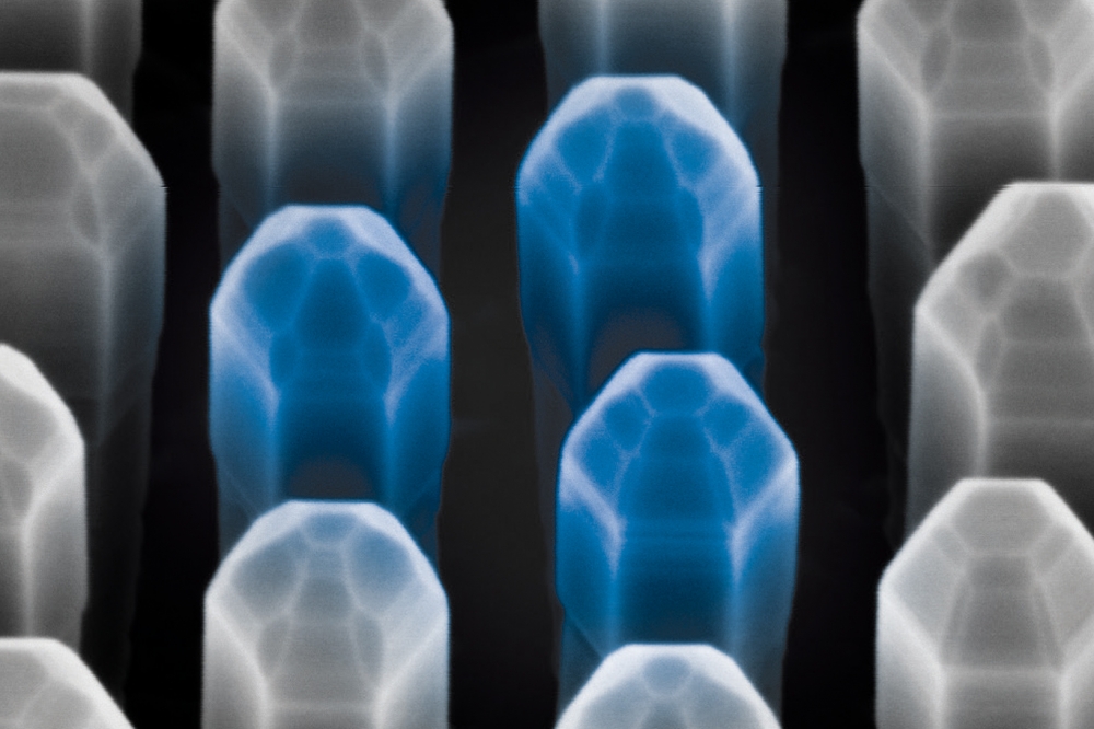
Figure 7. AlN nanowire (NW) sections are grown on an array of in-plane ordered GaN pillars, with a pitch of 800 nm. The upper section of the AlN NW section, shown in the right, is enlarged with respect to the GaN pillars, due to non-negligible lateral growth. It exhibits crystallographic facets associated with low surface energy planes.The polar plane corresponds to a (0001) facet and the non-polar plane to a (1100) facet.
Due to this great potential, we are now focusing on the development of deep-UV LEDs via the in-plane ordered approach. Our plan is to exploit the assets of MBE by combining its ability to control the growth of monolayer and sub-monolayer GaN quantum wells with the use of GaN templates grown by selective-area MOCVD (see Figure 7 for an array of such GaN pillars, and the AlN nanowire sections grown on top of them).
We are pleased to see that progress with MBE is popularising the use of 200 mm silicon substrates. Such an advance, drawing on the assets of MBE, in particular controlled growth of GaN quantum wells at the atomic scale, has the potential to change the paradigm of UV LED fabrication. The recent demonstration by Silanna of Brisbane, Australia, of layer-based UVC LEDs grown by MBE with a an impressive external efficiency of 0.8 percent at 235 nm is an illustration of the potential of this epitaxial technique and its capabilities to successfully compete with MOCVD. Our own target is to fulfil the promises of MBE-grown nanowire-based LEDs in the UVC range and take advantage of the fascinating properties of these miniature marvels.