Challenges for high-volume microLED manufacturing

Despite strong momentum, most microLED manufacturers are still experiencing delays in ramping volumes.
BY ERIC VIREY FROM YOLE INTELLIGENCE
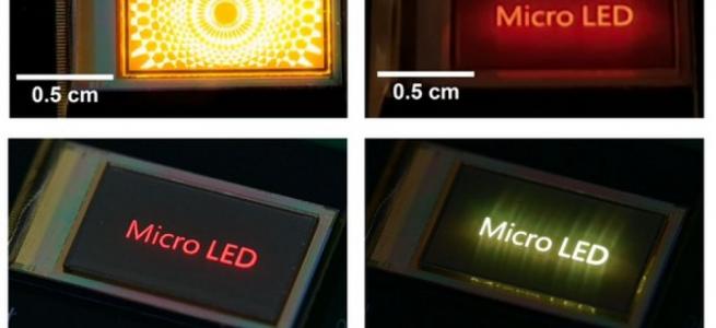
THERE ARE MANY great attributes of displays based on microLEDs, which are miniature red, green and blue emitters with dimensions typically less than 50 m. Thanks to independent control of every sub-pixel, displays based on microLEDs combine high-contrast, high-speed, and wide viewing angles – merits also found in OLED displays – with superior colours, better contrast, higher brightness, lower power consumption, longer lifetime, environmental stability and ruggedness. In addition, with microLED-based displays there is the possibility of integrating sensors and circuits, advances that would enable the production of thin displays with embedded sensing capabilities involving fingerprints, an in-display camera, a touch function and gesture control.
Spearheaded by efforts from Apple and others, microLEDs have generated tremendous excitement over the past decade. According to the MicroLEDs 2023 report by our team at Yole Intelligence, $12 billion has been spent on efforts associated with microLED development and industrialisation, and another $2.4 billion on mergers and acquisitions. While this is dwarfed by the building costs of OLED fabs since the mid-2000s, a expenditure totalling more than $100 billion, it’s indicative of strong momentum. All display makers now have sizeable microLED efforts and the first commercial products are on the market, including a number of AR headsets and a TV from Samsung. Expected to join this list in the spring is a luxury watch from Tag Heuer.

Figure 1. Cumulative investment in microLED development and
manufacturing. Taken from microLEDs report, Yole Intelligence, 2023.
Credit: Yole Intelligence
More products are sure to follow, as the supply chain shapes up and more companies invest in manufacturing capabilities. Making headlines on this front is Osram, which is spending a billion dollars to build an 8-inch microLED fab in Kulim, Malaysia, to serve Apple’s needs for an upcoming smartwatch. As one might expect, this is by no means the only microLED activity in Asia: Taiwanese holding company Ennostar is building a 6-inch fab; most leading display makers in China have aligned themselves with leading domestic producers of LEDs; and in Taiwan and South Korea, AUO and Samsung have started producing small volumes of smartwatch displays and microLED TVs, respectively. Some investments in microLED capability in China are substantial, with BOE spending $300 million to acquire a controlling stake in HC SemiTek, which is using the entire proceeds to build a 6-inch microLED fab, and Sanan is spending nearly $2 billion on a new fab, with $200 million earmarked for microLEDs. In addition, JBD has completed its construction of a $100 million, vertically integrated microdisplay fab near Shanghai, and Vistar has broken ground on a $413 million microLED display project.
However, progress is not keeping pace with schedules. Osram’s fab, initially slated to ramp in 2024, is now expected to start in late 2025; and while Ennostar’s first phase is on track for mid-2024, the second phase has been pushed back by one-to-two years, to 2026 or 2027. Note that these are by no means the only projects to experience delays. But why is it taking so long to bring microLEDs to consumers?
Mass transfer: a major hurdle
MicroLEDs are challenging. Making a display involves processing LED epiwafers into arrays of microLED chips, poised for transfer and integration into a heterogeneously integrated system incorporating LEDs, pixel-driving transistors, optics and so on.
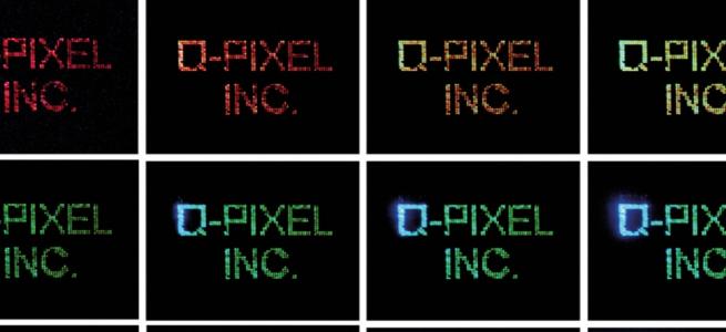
To manufacture a microLED display with an 8K resolution, which is 7680 pixels by 4320 pixels, requires the transfer and assembly of almost 100 million microLEDs with a placement accuracy of ±1 µm – and that must occur in less than 10 minutes to ensure economical viability. Unfortunately, today’s LED and die bonders are incapable of manipulating the very small die deployed in high-volume consumer applications, and at the required level of precision their throughput is typically limited to no more than around 1,000 die per hour. At this pace it would take 11 years to manufacture a single 8K TV. Recently developed miniLED transfer equipment trims this time, but it is still longer than a week.
What’s needed is a paradigm change: the development of mass transfer technologies that manipulate and assemble far smaller die at a rate five orders of magnitude faster.
The good news is that progress has been spectacular, to the point that many industry players no longer see it as a fundamental roadblock. Only three years ago, a company developing microLED displays had to invent its own mass transfer process and build its equipment. Now, more than a dozen off-the-shelf tools are available from equipment makers. These first-generation tools are suitable for development, pilot lines, and, in some cases, for a first product.
However, to ensure costs meet expectations, the microLED has to be shrunk below 10 µm. For example, the microLEDs that Apple will use in its smartwatch will be 6-8 µm. At those sizes, most tools struggle. Another challenge facing equipment makers is that their tools have to operate over large areas – at least 730 mm by 920 mm, and possibly up to 1500 mm by 1850 mm. These challenges associated with mass transfer are thought to be the culprit for Apple’s smartwatch manufacturing ramp delay. This tech giant is working with a partner to develop a custom tool based on its proprietary MEMS-based technology.

Figure 2. Required die assembly equipment capabilities for microLED vs.
existing LED and miniLED solutions. Taken from microLEDs report, Yole
Intelligence, 2023. Credit: Yole Intelligence
Yield and repair
Another factor to consider alongside transfer and assembly is yield, which has impact on cost. With microLEDs, bad (dead) pixels can originate from either a faulty die, a missed or misplaced die during transfer, or a defective electrical connection. Today, transfer yields range from 3N (99.9 percent) to 5N+. Meanwhile, microLED chip yields are between 99 percent and 99.5 percent.
While those numbers initially appear impressive, they equate to half a million defective pixels in an 8K TV. As the eye is incredibly sensitive to defects, manufacturers must develop effective yield management strategies that combine pixel redundancies and/or individual pixel repair with chip and pixel testing and binning.
To limit repair needs, it is critical for makers of microLED-based displays to use testing and inspection to remove bad die from the process flow as early as possible. Assisting in this endeavour are multichannel probe-card testing tools, but their workload is daunting, as it will not be long before there are 500 million die on a single 8-inch wafer. Even today’s best commercial probers would take more than 40 hours to test one of those wafers. A better option for very small high-density chips is massively parallel, contactless testing. A tool providing this form of testing has been introduced to market in 2023 by the Korean company Top Engineering, but its capability is still to be demonstrated in volume production. Note that in 2020 Apple acquired start-up Tesoro, with the aim of developing an in-house solution.

Figure 3. Yield and repair in microLED display manufacturing. Taken from
microLEDs report, Yole Intelligence, 2023. Credit: Yole Intelligence
As well as the need for tools and technologies for microLED mass transfer and massively parallel contactless testing, there are other challenges. They include the driving of the microLED displays, a task that requires innovation, as it is not possible to simply use the drivers of OLED displays. Another hurdle is to improve the external quantum efficiency of the microLED, which can plummet when scaled to very small dimensions.
One may view a microLED display as a new, complex puzzle. While many pieces already exist, some are yet to be perfected – and they need to be brought together, with the last few kinks ironed out, which will take more time. It is only after yields and costs get close to target that the first consumer products will appear. The next two-to-three years are going to be critical, with Apple’s smartwatch and Samsung’s TV projects acting as incubators for the entire industry. That watch is now expected in 2026, and if it fails, this would be a massive and potentially fatal blow.
Nevertheless, there is very strong momentum for the microLED. However, its innovators cannot let up, because the OLED keeps improving, so there’s a sense of urgency to accelerate commercialisation and secure some success before OLEDs get too entrenched in all major target applications.
Further reading
MicroLEDs 2023, Yole Intelligence
MiniLEDs 2023, Yole Intelligence
MiniLED Displays 2023 - Performance and optical construction, Yole Intelligence
Sony MicroLED display, Yole Intelligence