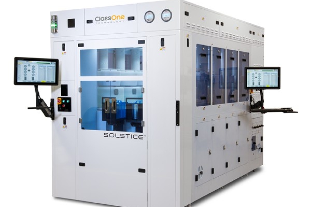
Porotech selects ClassOne Solstice tool
Plating capabilities to help advance GaN products for next-generation microLED microdisplays
ClassOne Technology has announced that Porotech, a UK-based pioneer in GaN-based microLED technology, has selected the ClassOne Solstice single-wafer platform for the development and manufacture of GaN products for applications requiring silicon wafer substrates.
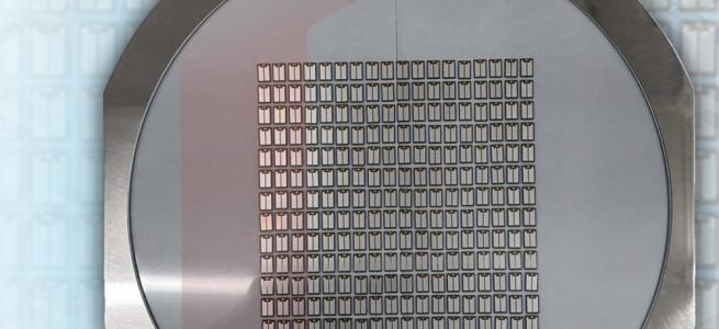
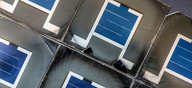
The devices being developed by Porotech target ultra-high-density and energy-efficient microLED microdisplays for augmented reality (AR) applications, wearables, and smart devices. Porotech has developed the PoroGaN GaN-on-silicon platform and Dynamic Pixel Tuning (DPT) microLED-on-silicon (µLEDoS) technology, which can be engineered to produce light at wavelengths across the visible spectrum.
“Porotech is tackling mass-production challenges with partners in the µLEDoS supply chain, integrating wafer manufacturing, hybrid bonding, IC design, packaging, and assembly solutions. ClassOne’s Solstice plating technology provides a reliable and efficient foundation for the development of key process steps that will support the route to improved yields through utilisation of larger silicon wafer sizes,” said Porotech CEO Tongtong Zhu. “We look forward to working with the team at ClassOne to bring the industry-leading performance benefits of PoroGaN and DPT to display applications in the next few years.”
ClassOne Technology CEO Byron Exarcos stated: “As a leading provider of plating equipment for microLEDs, we’re excited to participate in the development and growth of Porotech’s breakthrough, game-changing microLED technology and to help drive these solutions toward mass production and high-volume manufacturing.”
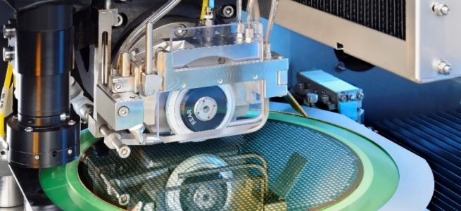
The Solstice single-wafer platform can combine multiple process technologies and chemistries in a single, small-footprint configuration for advanced chip packaging and surface preparation applications. Available with up to 3, 4 or 8 chambers, the scalable Solstice platform is suitable for both R&D and high-volume manufacturing environments, delivering ultimate wafer uniformity and process control. The system can also accommodate a wide variety of substrates, from traditional silicon devices to compound semiconductors and emerging materials such as glass.