Advancing the AlN Schottky barrier diode
Formed on native substrates, AlN Schottky barrier diodes offer a 3 kV blocking voltage and excellent performance at elevated temperatures
Engineers at Arizona State University are claiming to have produced the first AlN Schottky barrier diodes on single-crystal AlN substrates that can block 3 kV. These devices are said to offer excellent high-temperature performance and rectifying behaviours.
The team’s success is a noteworthy breakthrough. While AlN has much promise, thanks to its high critical field and its large Baliga’s figure of merit, the development of this class of power device is still in its infancy, due to challenges in material growth, contacts, doping, and fabrication.
“[Our] results show the potential of AlN as an ultra-wide bandgap semiconductor and represent a big step towards the development of multi-kV AlN high-voltage and high-power devices,” argues team spokesman Houqiang Fu.
He and his co-workers recent triumph builds on earlier work involving the production of AlN-on-sapphire diodes capable of blocking 1 kV. Switching to a native substrate has trimmed the defect density, which holds back device performance, including the blocking voltage.
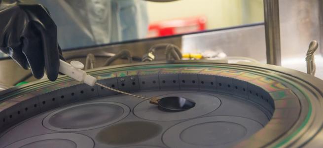
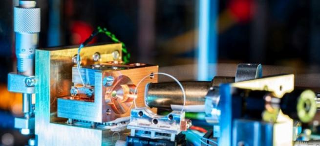
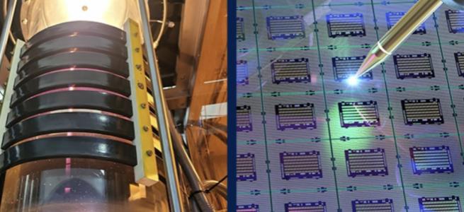
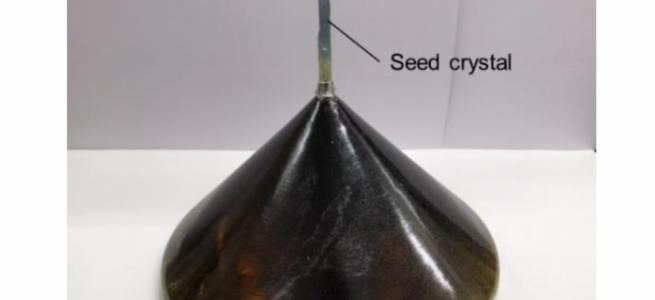
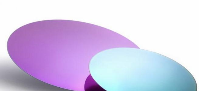
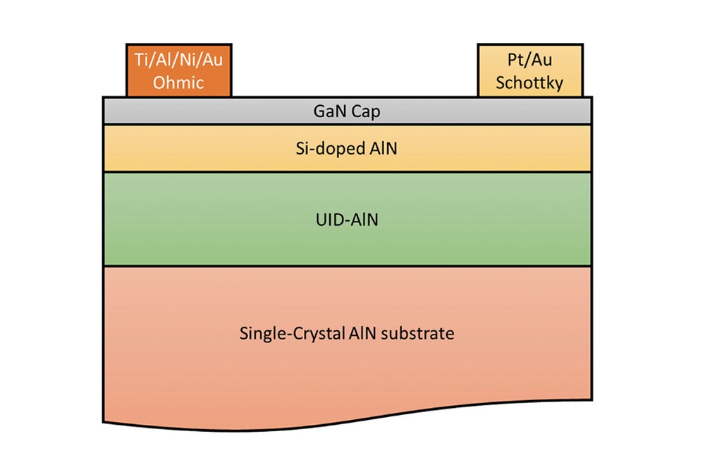
Production of the 3 kV Schottky barrier diodes began by loading bulk AlN substrates, produced by physical vapour transport, into an MOCVD reactor. On this foundation the team deposited a 1 mm-thick unintentionally doped resistive buffer, followed by a 200 nm thick AlN layer doped with silicon at a concentration of 1 x 1019 cm-3, and a 2 nm-thick unintentionally doped GaN cap.
To assess the crystal quality of the epilayers, the team considered the thickness of the peaks obtained by high-resolution X-ray diffraction. This suggest a dislocation density of 104 - 105 cm-2 – that’s three orders of magnitude below that for AlN grown on sapphire.
Following chemical cleaning of the epiwafers, the engineers fabricated Schottky barrier diodes using a conventional photolithography and lift-off process.
They produced a portfolio of devices, with the distance between the ohmic and Schottky contacts varying from 50 mm to 350 mm. None of the devices employed field plates, passivation, or edge termination structures.
Electrical measurements revealed on-off ratios of 105 - 106, and a turn-on voltage of around 2.5 V.
The team have also studied the ideality factor. A perfect device would have a value of 1, with values closer to this indicating a higher quality of the diode, due to fewer defects causing trap states at the metal-semiconductor interface. As the distance between the ohmic and Schottky contacts increased, the ideality increased from 4.29 to 7.52. This led the team to deduce that current transport is likely to be influenced by surface states and/or the resistance of the AlN epilayers due to a relatively low carrier concentration.
Increasing the temperature of the diodes with the best ideality factor from 298K to 623K revealed good temperature stability. With increasing temperature, the on-off ratio increased from 106 to 108, the Schottky barrier height went up from 0.89 eV to 1.85 eV, and the ideality factor fell from 4.29 to 1.95.
Reverse-bias measurements reveal that regardless of the distance between the ohmic and Schottky contacts, the diodes are capable of blocking 3 kV, the limit of the team’s apparatus.
One of the next goals for Fu and co-workers is to improve the reverse and forward electrical performance of their high-voltage AlN power diodes.
For reverse performance, efforts will focus on incorporating edge termination techniques, such as field plates, and introducing surface passivation. It’s hoped that this will trim the reverse leakage current and boost the breakdown voltages to 10 kV.
“For the forward performance, we will continue to improve the ohmic and Schottky contacts, to enhance forward current conduction and reduce on-resistance through surface treatment and optimised thermal annealing,” adds Fu.
Reference
D. H. Mudiyanselage et al. Appl. Phys. Express 17 014005 (2024)