How to integrate silicon and III-Vs
To draw on all the traditional benefits that come from scaling, silicon
and the III-Vs must be united via epitaxy and processing in silicon
foundries.
BY EUGENE FITZGERALD, FAYYAZ SINGAPOREWALA, DANIEL LEPKOWSKI AND JOHANNE CHU FROM NEW SILICON CORPORATION
THE MAINSTREAM semiconductor industry is continuing to head in the same direction. The focus, as always, is the miniaturisation of the silicon transistor. Success on this front today allows more of them to be packed on an IC, making this chip more powerful. It’s an approach that enhances the capability of memory and computation but is expected to lead to commoditisation as this industry continues to mature.
In addition to scaling, the silicon industry is exploring other directions. That includes the integration of silicon with compound semiconductors, a marriage that has much promise as it offers the opportunity to draw on the best of both worlds. There is the tantalising prospect of combining the low cost, impressive toolsets and high volumes of the silicon industry with the prowess of the compounds, which include powerful light emission, high blocking voltages, and efficiency and power in the RF domain.
It is crucial that when the compounds are united with silicon, the strengths associated with the latter technology are retained. Occupying the top spots of this valued list are the need for high-density devices, enhanced performance from scaling, and cost reduction.
Historically, increases in device density have been a major driver behind improvements to microprocessors, multicore processors and silicon memory. In the future, high transistor and LED densities will be needed in augmented-reality displays accommodating millions of pixels, as well as pixelated light sources and highly efficient single-chip phased arrays.

Figure 1. Cost per interconnection versus interconnection density.
Custom silicon and silicon gate array are monolithic silicon chips (BEOL
of CMOS is interconnecting high-density transistors). When interconnect
(and therefore device) density at the chip level decreased to
approximately 10,000 per square inch in 1984, costs favoured the
fabrication of longer interconnects at the board/package level. [Adapted
from W.H. Knausenberger and L.W. Schaper, “Interconnection Costs of
Various Substrates- The Myth of Cheap Wire”, IEEE Transactions on
Components, Hybrids, and Manufacturing Technology, vol. CHMT-7, pp.
261-263, September 1984.]
In general, scaling has excelled in increasing the ‘bang’ while lowering the ‘buck’. Miniaturisation can be credited for higher circuit frequencies, lower power consumption, lower parasitics, reduced noise and superior heat removal. It’s forecast that these performance enhancement benefits from miniaturisation will continue, with possible new dimensions for the digital control of arrays of high-density devices, such as LEDs and HEMTs.
The trimming of costs that come from scaling are not just due to an increase in the number of circuits per area, ensuring a reduction in the cost to produce each circuit. There is also the average cost for the interconnects between devices to consider – this depends on the interconnect length, with shorter interconnects more cost-effective.
Since the 1980s, the economics of monolithic integration at the chip level have been understood (see Figure 1, which demonstrates the relationship between interconnect density, cost per interconnection, and device density). We have come a long way since 1984, when interconnect density was below 10,000 per square inch and it made economic sense to have interconnects at the board/package level, rather than at the chip level. Over the intervening years, there has been the introduction of more and more wiring levels in chips, and interconnects have migrated from the board or package level to the chip level.
As well as the three strengths just outlined – the new chip possibilities, enhanced performance and cost reduction – there are others associated with silicon manufacturing that should be retained when compound semiconductors are brought onboard. These merits include a high yield, a high level of reliability, and speedy product design cycles.
Yield and reliability have undergone steady improvement, due to the use of the same fabrication process for multiple products. A high yield is also aided by low-cost self-diagnostic capabilities for in-line and post-processing measurements – these are features that are facilitated by the integrated design process.
Another asset is the use of a common silicon wafer manufacturing process, which increases the volume of products passing through the process, and drives improvements to yield, reliability, and cost-effectiveness. Crucially, despite the common approach, each customer retains their own design intellectual property.

Figure 2. The line across the graph represents the historic increase in
the density of transistors over time. Superimposed are LED densities in
current and future LED display products. With monolithic silicon
integrated circuit manufacturing of CMOS + GaN LEDs, microdisplays will
be single-chip and manufactured in silicon fabs.
Integration with LEDs
One attractive opportunity for integration involves the creation of a single-chip LED display, formed by using millions of transistors to drive and address millions of LED pixels. In this case, the LED density in these displays is comparable to the density of transistors in early microprocessors. Due to this, as was the case with those microprocessors, it makes little sense to package all these components together, because it is not feasible to achieve such density, the cost is too high, and such an approach would negate the advantages, in terms of yield and reliability, that come from monolithic integration.
It is possible to compare the density of LEDs in a range of products, including wearables, virtual reality and augmented reality, with historic transistor densities (see Figure 2). This plot shows that the manufacturing of LED displays can be disrupted when LEDs become part of silicon manufacturing and are interconnected with CMOS using the CMOS back-end-of-line (BEOL) approach. Note that arguing against such a trend is as nonsensical as suggesting that the Pentium processor should have been constructed by packaging individual transistors together, such as through mass-transfer or pick-and-place techniques.
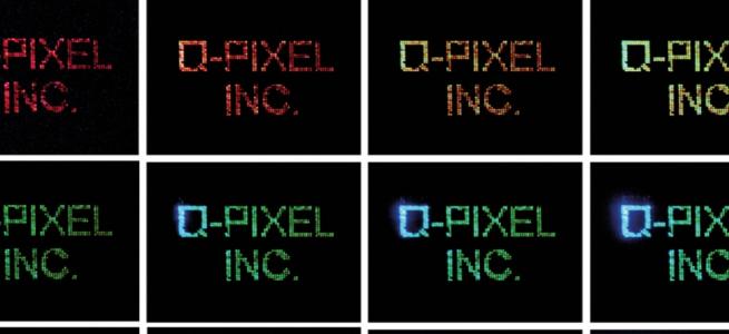
To support the advance of single-chip displays, our team at New Silicon Corporation, Singapore, has developed the necessary materials, processes, structures, devices, and software design modules to create integrated circuits using silicon integrated circuit manufacturing that can unite CMOS devices and GaN-based LEDs. Our first set of products will be white or monochrome LEDs, the latter available in red, green and blue. For red and green variants, emission will result from blue light that pumps quantum dots. Further ahead, we plan to produce integrated full-colour displays, with quantum dots present on the red and green pixels.
Our CMOS + III-V process consists of three stages (see Figure 3): CMOS front-end of line (FEOL), new III-V FEOL, and CMOS BEOL. The first and last stages are taken directly from standard silicon CMOS manufacturing, which produces complete circuits by connecting transistors with a FEOL process on silicon wafers using a multi-level metal interconnection network formed in the BEOL. For our CMOS + GaN LED process, we sandwich a GaN FEOL between the CMOS FEOL and BEOL. After GaN LEDs are fabricated, the BEOL’s interconnection network connects CMOS transistors and LEDs to create a monolithic integrated circuit. The silicon CMOS BEOL serves as the interconnection network for both silicon and III-V devices. It’s an approach that enables an integrated design environment using standard integrated circuit design software.
A tremendous benefit of adopting the silicon front-end and back-end processes for III-V devices is that each mask is aligned to the former one, guaranteeing yield and reliability across the wafer. In addition, this approach eradicates problems that arise when fabricating silicon transistors and III-V devices separately, and then trying to use wafer-scale metallic bonding and alignment to interconnect the devices. When III-V devices are on a separate wafer, realising high-density alignment across the two types of wafers with different materials stacks and thermal expansion coefficients is problematic and low yielding, especially at 200 mm or larger wafer sizes.
Another challenge when uniting III-Vs and silicon is optimising the usable wafer area across both device layers. When wafer bonding is employed to combine silicon die and III-V die, the area occupied by III-V devices is not the same as that occupied by the silicon circuits. Consequently, the unused area on a wafer – often the III-V wafer – is required to spread out circuit components for alignment to the other die on the wafer. This is far from optimal, as it decreases the effective chips per area and increases cost. Unfortunately, this fundamental cost and design constraint is often overlooked, and the limited use cases and higher costs that follow are a headwind to potential wafer sales volumes, further increasing the cost-per-wafer for wafer-bonding approaches.
A far better approach is true monolithic integration. Using sequential masks, as is the case in silicon integrated circuit design and manufacturing, we use integrated circuit designs that intermix silicon and III-V devices. This approach enables the most compact area and the most efficient design, both for circuits and for chips. As all designs employ the same process, wafer volume is maximised, helping to ensure the lowest cost per wafer.
One crucial step in our monolithic process is the transferring of the CMOS FEOL onto a GaN-on-silicon epiwafer. After the transfer, the CMOS FEOL remains on the wafer’s surface, resembling a regular CMOS wafer. The GaN LED epitaxy beneath the CMOS FEOL surface is hidden, but the processing of GaN LEDs in specific areas is still possible, by etching through the top thin surface of silicon that hosts the CMOS FEOL.

Figure 3. The monolithic process for creating CMOS + III-V circuits
begins by processing III-V devices on the same wafer as the silicon
transistors, after the silicon transistors have been processed. With the
silicon process strategy of sequential masks, each aligned to the one
before it, is critical for a processing platform to gain the benefits of
integration and miniaturisation across many product segments. (a) A
standard silicon FEOL is fabricated, according to the design, in a
foundry and transferred onto a III-V-on-silicon epitaxial wafer. (b)
III-V device FEOL is done, automatically aligned to silicon FEOL via
sequential masks. (c) Sequential masks form the silicon BEOL, which
interconnects the silicon transistors and III-V devices according to
circuit design. Diagrams are not to scale or proper aspect ratio.
With our approach, the areas reserved for LED fabrication must be kept separate from CMOS components. This is accomplished by incorporating III-V device models into the standard CMOS design kit that’s provided by the foundries that provide the FEOL and BEOL services. The development of a process design kit (PDK) is crucial for bridging the gap between integrated circuit design and semiconductor foundries for chip fabrication.
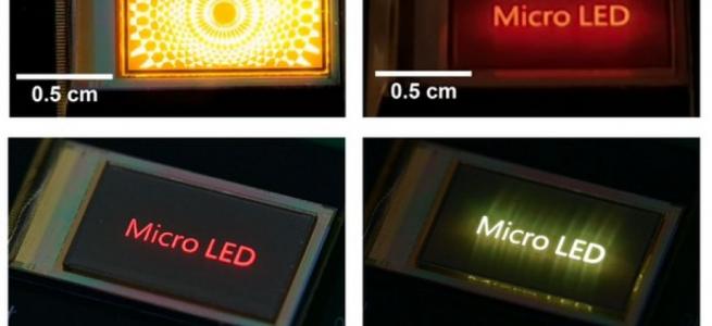
We have developed an integrated CMOS + GaN PDK that provides comprehensive solutions for large-scale circuit simulation, design, and layout verification. This PDK allows for circuit design and fabrication on our proprietary integrated CMOS + GaN wafer technology. Our PDK libraries are specifically tailored to our CMOS + GaN offerings, and they cater for unique applications that are outside the scope of the portfolio of conventional CMOS or GaN foundries. Thanks to close collaboration between the process development and IC design teams, we have carefully fine-tuned every aspect, thereby ensuring a robust, reliable bridge between integrated circuit design and fabrication. Our efforts will provide the catalyst to a new era of chip-based solutions for displays, lighting, and wireless systems, overcoming the challenges of III-V-on-silicon integrated circuit design and fabrication (see Figure 4 for an example of a processed 200 mm CMOS + GaN LED circuit).
So far, we have focused on rolling out our initial platform, the CMOS + GaN LED platform. However, our monolithic integrated circuit process can be applied to any CMOS + X platform, where X could be a III-V, or another semiconductor material or device. For integration, it is essential that: there is the capability to produce epitaxial device layers on silicon wafers with an appropriate diameter for silicon line manufacturing; and the defect density in these epitaxial device layers is low enough to ensure and maintain a satisfactory performance in the final integrated devices in the circuit throughout the product lifetime.

Figure 4: A transmission electron microscopy cross-section of a finished
200 mm wafer processed using silicon foundry manufacturing. The
tungsten plug process used for the BEOL is used to also connect to the
III-V FEOL.
As we ramp production of digitally controlled power amplifiers, we are preparing for the introduction of our next product: single-chip phased arrays for 5G/6G. Faster data rates have led to increases in wireless communication frequencies, which has had the downside of higher degrees of absorption in the atmosphere. Due to this, there’s a need to focus the transmission of high-frequency wireless signals on the cell recipient station. In the infrastructure of yesteryear, this would have been accomplished with movable dish antennas. However, that’s not feasible in consumer devices. In the likes of the smartphone, one way to electronically steer the wireless beam towards the receiver is to use a chip populated with multiple GaN HEMTs, precisely arranged at specific distances from each other on a plane. We view these single-chip phased arrays, manufactured at lower costs in silicon fabs, as crucial for expanding the deployment of high-bandwidth consumer wireless systems.
There is no doubt that the integration of III-V materials and devices into silicon integrated circuits is opening up entirely new market segments for the silicon industry. For that industry, the monolithic integration of new devices into silicon systems will define the next stage of growth, driven by miniaturisation, integration, and scaling of integrated circuits. This will create new high-growth markets, targeted by high-performance systems produced at very competitive costs.
Our immediate focus is the microLED illumination and display market. According to analysis by Spherical Insights and Straits Research, this market had a value of $650 million in 2022, and is forecast to climb at a compound annual growth rate of more than 80 percent through to 2030, when it will be worth $36.5 billion. Demand is driven by the desire for brighter, more powerful display panels for consumer electronic devices, including high-end smartphones and wearable displays, such as head-mounted devices.