Extreme-temperature devices using AlN
Diodes and transistors with AlN channels deliver high breakdown voltages and operation at incredibly high temperatures.
BY HIRONORI OKUMURA FROM UNIVERSITY OF TSUKUBA
A NUMBER OF human activities are expanding into extreme environments, often motivated by resource exploitation. This has taken exploration in various directions, including deep underground, to great depths at sea and into deep space. In all these environments the temperature is extreme – it exceeds 300 °C on the surface of Venus, in deep-well drilling, and in the space inside an operating engine.
To find out more about all these environments demands the deployment of sensors. But the most obvious ones – that is, those based on silicon – are not up to the task, due to a relatively low operating temperature limit. This means that in order to enrich our lives from these environments, we need to develop extreme-temperature electronics.

Figure 1. The leakage current path and the thermal degradation points in a MESFET with a gate oxide.
When all forms of semiconductor device are operated at extreme temperatures, they face issues associated with materials, electrodes, gate oxides and packaging (see Figure 1). As the temperature increases, numerous electron-hole pairs are generated, due to excitation of electrons from the valence band maximum to the conduction band minimum. These electrons, which increase the intrinsic-carrier concentration (see Figure 2 (a)), are detrimental, as they increase the leakage current of the devices and prevent them from turning off. Options for reducing the leakage current include introducing semiconductor materials with a larger bandgap energy and lower intrinsic carrier concentrations (see Figure 2 (b)), or restricting current diffusion from areas other than the channel. Turning to a channel layer surrounded with high-resistivity layers that have low effective donor/acceptor concentrations and low defect concentrations can raise the device’s operating temperature. Another approach is to deploy devices with p-n junctions, such as JFETs and BJTs. In these cases, it’s also important to select refractory metals for the electrodes that have minimal reactivity with base semiconductors. In particular, titanium, vanadium, tantalum, molybdenum, tungsten, and platinum are better for this purpose than aluminium, magnesium, copper, silver, indium, and gold.
Why use AlN?
There are many semiconductor materials with a larger bandgap energy than silicon. They include SiC (3.3 eV), GaN (3.4 eV), Ga2O3 (4.7-5.2 eV), diamond (5.5 eV), and AlN (6.1 eV). The team at NASA, led by Philip Neudeck, have reported that SiC JFETs can operate at temperatures over 800 °C. While this is undoubtedly an impressive result, materials with even wider bandgaps promise to reach even higher temperatures. However, quite a few of them have significant drawbacks. GaN suffers from a high effective donor concentration of 1016 cm-3; it’s not possible to form p-type Ga2O3 layers; and diamond starts to reacts with oxygen at around 700 °C. In stark contrast, AlN has no obvious flaws, and offers thermal stability and controllable doping. Due to these attributes, our team at the University of Tsukuba has been devoting all our attention to AlN for the development of extreme-temperature devices.
Historically, it’s been assumed that AlN is only good as an insulator. However, around 20 years ago Yoshitaka Taniyasu and colleagues at NTT demonstrated that this is not the case by growing electrically conductive AlN layers by MOCVD.
This team recorded an electron mobility of 426 cm2 V-1 s-1 for silicon-doped AlN layers, for a dopant concentration of 3 x 1017 cm-3. Building on this work, they went on to pioneer p-type AlN growth and demonstrate the first AlN LEDs with a wavelength of 210 nm and quasi-vertical AlN p-n diodes. These successes are to thank for the recent, rapid development of deep-UV LEDs based on AlGaN and AlN.

Figure 2. (a) An illustration of electron-hole pair generation at high
temperatures. (b) The intrinsic carrier concentration of silicon, SiC,
GaN, β-Ga2O3 diamond, and AlN as a function of reciprocal temperature.
As well as optical devices, the research community has investigated AlN Schottky barrier diodes and AlN/AlGaN HEMTs, to explore the potential benefits of a high critical electric field. Unfortunately, these devices suffer from a low carrier concentration, due to high ionization energies for the donors and acceptors – it is 0.3 eV for silicon and 0.6 eV for magnesium. Due to this, carrier concentrations for both these dopants are around two orders of magnitude lower than their concentrations, causing devices to have very small currents. To overcome this problem, our team, in working in partnership with researchers at MIT and Aalto University, have broken new ground by introducing polarisation-induced doping in N-polar AlGaN/AlN structures. Thanks to spontaneous and piezoelectric polarisations, this form of doping can increase current and lower contact resistivity. Using polarisation-induced doping, we have demonstrated the first N-polar AlN-based PolFETs and HEMTs with drain currents over 100 mA mm-1. Such success has led us to view AlN as a practical semiconductor for optical and electrical devices.
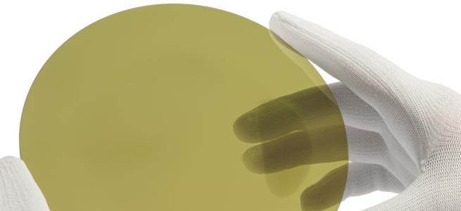
To produce these devices, we have been able to draw on a number of material suppliers. High-quality AlN samples on 2-inch sapphire substrates can be purchased from Dowa Electronics Materials, and 2-inch bulk AlN is commercially available from Stanley and Asahi Kasei.

Figure 3. (a) Depth profiles of the impurity concentration of silicon,
oxygen, and carbon in a 3 µm-thick silicon-implanted AlN layer after
annealing at 1600 °C. (b) Depth profiles of the magnesium concentration
in a 1 µm-thick, magnesium-implanted AlN layer after annealing.
Doping AlN
Controlling the concentration of dopants in semiconductors is the incorporation of impurities during crystal growth, as well as thermal diffusion and possibly implantation. The latter is an attractive technology, enabling precise dose control and ensuring a high lateral uniformity of the dopant. However, when high-dose implantations are employed, they tend to damage crystal lattices and introduce high concentrations of point defects, which can compensate carriers. Fortunately, most of this damage can be repaired with post-thermal annealing, which we have used when producing a silicon-implanted n-type AlN channel.
One of the impressive traits of AlN crystals, including their surfaces, is a robustness at elevated temperatures, with stability under nitrogen gas at up to 1700 °C. This robustness provides a wide window for repairing implantation damage – this process requires temperatures above 1200 °C for electrical activation of the silicon-implanted AlN layer. Note, though, that much thought is needed when selecting the annealing temperature, as it can drive other changes in the material. Beyond 1400 °C, silicon and oxygen impurities diffuse within the layer above. Due to diffusion of oxygen atoms from the sapphire substrate, which decomposes at 1500 °C under nitrogen gas, a thin AlN layer on a sapphire substrate will have a high oxygen concentration after high-temperature annealing, leading to degraded electrical characteristics.

Figure 4. (a) The cross-section of a Schottky barrier diode with a
silicon-implanted AlN channel. Ni/Au anode and Ti/Al/Ti/Au cathode. (b)
Current density-voltage characteristics of an AlN Schottky barrier diode
from 27 °C to 827 °C.
Through collaboration with MIT, Aalto University, TNSC, and Dowa Electronics Materials, we have investigated the diffusion of silicon, oxygen and magnesium atoms in AlN (see Figure 3). Our investigations revealed that oxygen atoms diffusing from a sapphire substrate cannot reach the channel layer after annealing by using 3 µm-thick AlN layers. This led us to conclude that the preferred annealing temperature ranges for electrically conductive AlN layers with silicon and magnesium implants are 1200-1600 °C and 1400-1500 °C, respectively. This knowledge enabled us to demonstrate the first AlN-channel transistors.
When the fabrication of devices involves conditions close to thermal equilibrium, such as epitaxial growth and high-temperature annealing, the formation of deep states with ionization energies of 250-320 meV is favoured. This tends to lead to self-compensation of the silicon donor, a situation in agreement with our results.
Meanwhile, the use of non-equilibrium processes, such as ion implantation, enables an increase in the population of shallow donors with ionization energies of 64-86 meV. This led Hayden Breckenridge and colleagues at the University of North Carolina and Adroit Materials to produce a highly conductive layer of AlN by silicon implantation and post-annealing at a relatively low temperature of 1200 °C. Another encouraging result, coming from Kyoto University, is that the substitutional magnesium-acceptor binding energy of AlN is only 250-410 meV, a value much smaller than the ionization energy of magnesium acceptors in common MOCVD-grown AlN layers. Taken together, these results indicate that if non-equilibrium process conditions can be reproducibly and easily controlled in AlN that’s doped with silicon and magnesium, this could open the door to electronic and optical devices with significantly improved performance.

Figure 5. (a) Schematic cross-section of MESFET with a silicon-implanted
AlN channel. (b) DC output characteristics of an AlN MESFET at 727 °C.
Electrical properties of AlN
To improve the electrical performance of AlN-based devices, there is more to do than just address the high resistivity of n-type and p-type AlN layers that are impaired by low carrier concentrations. In addition, there’s a need to tackle the high contact resistivity, resulting from the small electron affinity.
It is particularly challenging to make an ohmic contact at room temperature in AlN. The voltage drop is governed by the height of the Schottky barrier, which depends on the difference between the metal work function and the semiconductor electron affinity. It is possible to produce ohmic contacts by lowering the potential barrier height through appropriate selection of electrode materials. Options for n-type AlN are titanium, aluminium, vanadium and molybdenum, while ohmic contacts to p-type AlN can use palladium and NiO.
One implication of heavy doping in semiconductor materials is a decrease in the depletion-region width, leading to tunnelling through potential barriers. The heavy doping of the topmost AlN surface is very important for ohmic contacts. However, as the concentration of silicon and magnesium dopants in AlN layers is limited to around 1019 cm-3, perhaps due to the formation of compensation defects, there is no prospect for field-emission tunnelling.
To determine the carrier concentration and carrier mobility in semiconducting structures, researchers tend to turn to Hall-effect measurements. As these measurements need ohmic behaviour, some studies have used heavily doped GaN contact layers. This enabled the determination of the electrical properties of AlN, both at room temperature and at elevated temperatures. Along with others, we have evaluated the carrier concentration and carrier mobility at high temperatures, obtaining values for n-type and p-type AlN at temperatures beyond 200 °C and 500 °C, respectively.

Figure 6. A benchmarking plot, comparing the current on–off ratio versus
measurement temperature of AlN devices with the other state-of-art (a)
Schottky barrier diodes and (b) FETs.
When undertaking this study, we uncovered a new problem associated with high-temperature measurements. We had to use a probe station, as we lacked bonding and package technologies for extreme temperatures. We also found that normal probe tips deteriorate at high temperatures. Note that most reported devices have a maximum operating temperature of no more than 500 °C, implying that measurements of electrical properties are unreliable at temperatures higher than this.
Working with Dowa Electronics Materials, we have evaluated the electrical characteristics of 3 µm-thick AlN layers on sapphire substrates with a high-temperature probe system offering a maximum measurement temperature of 900 °C in high vacuum. For this effort we implanted silicon in the AlN layer at room temperature to obtain n-type conductance; the concentration was 2 × 1019 cm-3 in a 150 nm-deep box profile. These silicon-implanted AlN layers were subsequently annealed at 1500 °C. We then deposited Ti/Al/Ti/Au electrodes for ohmic contacts, prior to sintering at 950 °C.
Our electrodes deteriorated at 877 °C, possibly due to a reaction between Ti/Al and AlN. This led us to seek suitable metals for ohmic contacts at extreme temperatures. For the temperatures we were able to consider, we observed a current-voltage relationship that’s non-linear below 127 °C and almost linear above 227 °C. Evaluating electrical properties between 227 °C and 827 °C revealed that sheet resistance and contact resistivity decreased with increasing temperature. From 227 °C to 627 °C, as the temperature increased electron mobility slightly fell, but the electron concentration increased due to enhanced donor ionization, resulting in a reduction in sheet resistance at high temperatures. This led us to conclude that n-type AlN layers exhibit excellent performance at extreme temperatures.
Diodes and transistors
We have fabricated Schottky barrier diodes and MESFETs with silicon-implanted AlN layers on sapphire substrates. Our diodes are capable of operating at 827 °C (see Figure 4), surpassing all previous records, while our transistors can operate at up to 727 °C (see Figure 5). The AlN Schottky barrier diodes have a breakdown voltage of 610 V at room temperature, while the corresponding value for the AlN MESFETs at 727 °C is 176 V. We are keen to point out that these devices are practically feasible, because they have a simple structure, and the AlN layers are grown on large, low-cost sapphire substrates.
To fabricate our Schottky barrier diodes and MESFETs, we used Ni/Au for the anode and gate contacts. We found nickel to be thermally stable, hardly reacting with AlN, even at 827 °C. What’s more, in terms of electrical characteristics, we found little difference between Ni/Au and Pt/Au. For the Schottky barrier diode, the off current is small, even at 827 °C, due to the low intrinsic carrier concentration and the thermally stable Ni/AlN interface. However, the off-state drain current of the AlN MESFET is high at 727 °C, due to leakage through the bottom undoped AlN layers and the high concentration of defects. Unlike the current in silicon devices, which falls at high temperatures due to phonon scattering, we discovered that the forward current of AlN Schottky barrier diodes and MESFETs continues to increase with temperature up to 827 °C. We attribute this to the current in AlN devices at extreme temperatures being dominated by the increase in electron concentration and the reduction in contact resistivity, with the reduction in electron mobility playing a secondary role.
Our development of AlN devices is paving a new way to making semiconductor devices that can operate at extreme temperatures. Although there is a trade-off between the on-off ratio and the temperature of Schottky barrier diodes and FETs (see Figure 6), AlN devices have much potential for improvement. For example, it should be possible to increase the on/off ratio at extreme temperatures through a combination of homoepitaxial growth and the introduction of a JFET structure. Additional improvements could come from the introduction of heat-tolerant ohmic contacts, rather than Ti/Al/Ti/Au, a move that would increase the operating temperature to over 877 °C.
For most extreme-temperature applications, ICs need to operate reliably over long periods. Such circuits are fabricated with complementary technology, with n- and p-channels. At Kyoto University, engineers have developed a SiC complementary JFET logic gate that operates at 350 °C. We hope to take our work in a similar direction, producing complementary JFETs with homoepitaxial AlN channels that are capable of operating in extreme environments.
Further reading
Y. Taniyasu et al. “An aluminium nitride light-emitting diode with a wavelength of 210 nanometres” Nature 441 325 (2006)
P. G. Neudeck et al. “Demonstration of 4H-SiC Digital Integrated Circuits Above 800 °C” IEEE Elec. Dev. Lett. 38 1082 (2017)
H. Okumura et al. “AlN metal–semiconductor field-effect transistors using Si-ion implantation” Jpn. J. Appl. Phys. 57 04FR11 (2018)
J. Lemettinen et al. “N-Polar Polarization-Doped Field-Effect Transistor based on AlGaN/AlN with drain current over 100 mA/mm” IEEE Elec. Dev. Lett. 40 1245 (2019)
A. G. Baca et al. “Al-rich AlGaN based transistors” J. Vac. Sci. Technol. 38 020803 (2020)
M. Hayden Breckenridge et al. “Shallow Si donor in ion-implanted homoepitaxial AlN” Appl. Phys. Lett. 116 172103 (2022)
M. Hiroki et al. “High-Temperature Performance of AlN MESFETs with Epitaxially Grown n-Type AlN Channel Layers” IEEE Elec. Dev. Lett. 43 350 (2022)
H. Okumura et al. “Impurity diffusion in ion implanted AlN layers on sapphire substrates by thermal annealing” Jpn. J. Appl. Phys. 61 026501 (2022)
H. Okumura et al. “Mg implantation in AlN layers on sapphire substrates” Jpn. J. Appl. Phys. 62 020901 (2023)
H. Okumura et al. “Temperature dependence of electrical characteristics of Si-implanted AlN layers on sapphire substrates” Appl. Phys. Exp. 16 064005 (2023)