A sound approach to cutting costs
The harnessing of acoustic energy promises to enable substrate re-use during the production of wide bandgap power electronics.
BY ARNO MERKLE FROM CRYSTAL SONIC
There’s no doubt that compound semiconductor devices are on a long-established upward trajectory. Even as far back as the end of the twentieth century they were playing a number of crucial roles in our lives: they were a key ingredient in telecommunication networks; they were providing the optical source for the CD player; and they performed two essential roles in handsets – lighting keypads and amplifying RF signals. During the last two decades sales of these devices have continued to climb, due in part to deployment in lightbulbs and chargers. And growth is sure to continue, as revenues ramp through the electrification of transportation, the roll-out of 5G and the launch of countless satellites.
However, despite great performance advantages that have driven the success of compound semiconductor devices, their potential is yet to be fully realised. Holding this back are three related constraints in the manufacturing supply chain: a large demand-supply gap, particularly for wide bandgap devices based on SiC and GaN; high cost; and waste. Let’s analyse these three issues, one by one.

Figure 1. Sonic Lift-off workflow, enabling substrate re-use for wide bandgap materials.
First, there is a large and increasing gap between the demand for wide bandgap devices and their supply. For example, the Canaccord Genuity Group estimates that the demand for SiC-based power devices, driven by thirst for the likes of electric mobility, charging stations, industrial motors and solar inverters, is leading to approximately a three-fold shortage in SiC wafer supply over the course of this decade.
Second, wide bandgap materials are costly to produce, due to the inherent difficulty required to produce high-quality wafers with limited crystalline defects. Unlike silicon, crystals of GaN and SiC cannot be grown from the melt, leading to the need for a far higher energy input and greater challenges for process control. Another factor at play is that the industrial know-how for producing such materials, while broadening somewhat, is still relatively concentrated, especially for GaN and AlN. Due to these difficulties, it’s not surprising that the substrate prices for GaN, AlN and SiC are at least one or two orders of magnitude higher than those for silicon. As a result, their cost can account for about half of total device manufacturing cost – and this is not expected to appreciably change. Forecasts by PGC Consultancy indicate that wide bandgap substrates will remain the dominant manufacturing cost contributor, bottoming out at around 35-45 percent of SiC die cost in the coming decade as wafer production ramps up.

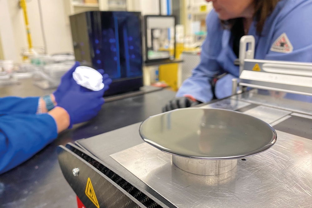
Figure 2. 4-inch GaAs wafers split by Sonic Lift-off, at Crystal Sonic laboratories in Phoenix, Arizona.
Third, waste in semiconductor manufacturing is abundant. Typically, discussions on this topic focus on either water waste and recycling strategies, or ways to limit the use of toxic chemicals, gases, and other consumables during chip manufacturing. But this strategy overlooks a more basic issue: waste of the wafer material itself. This really matters, as it’s not uncommon to waste at least 95 percent of wafer material during today’s conventional manufacturing process. With quite some effort, this material is literally ground into dust during two key steps in the manufacturing process. The first time this happens is during the slicing of large boules of wafer-grade crystals into wafers with a wire-saw, which is essentially a glorified bread slicer. During this step, known as ‘wafering’, approximately 50 percent of the material is lost to sawdust. The second step that wastes a great deal of material is the processing of wafers into chips, when they are typically thinned by mechanical back grinding. In this case, a sanding device provides ‘device thinning’, a step that eliminates up to another 90 percent of the substrate material, again to dust.
Over the past decade attempts to improve wafering have emerged that move beyond wire-sawing. These approaches, including those involving lasers, are capable of decreasing the waste associated with this step by around 50 percent. However, it is still challenging to reduce waste at the thinning step. While various attempts have been made, there are no lasting solutions that are suitable for producing wide bandgap bulk substrates of the highest quality.

Figure 3. Current-voltgae (I-V) plots for devices grown on 2-inch GaAs
(control-Red), after Sonic Lift-off (blue) and a regrowth on the
remainder substrate (green). Device performance comparison between
growth on a pristine substrate (red), a Sonic Lift-off device (blue) and
re-growth on a re-used substrate (green). All device growth done by
Rochester Institute of Technology and supported by DoE under contract
number DE-EE0008973.
A sound solution
At Crystal Sonic of Phoenix, AZ, we are breaking this deadlock with a novel technology that’s based on the use of sound energy. With this approach we are opening the door to thin device lift-off and substrate re-use, overcoming barriers encountered by previous efforts in this domain.
Our technology provides a pathway for simple, multiple wafer reuse that reduces the substrate cost proportionally with the number of wafer reuses. To deliver these savings, we combine a removable stressor that defines the depth of the cut with a highly tuneable acoustic source (see Figure 1 for an illustration of how our patented technology harnesses the power of sound to separate thin devices from semiconductor substrates, thus enabling substrate re-use).
A key advantage of our approach is that a crack front is guided smoothly through a substrate at a controlled speed. This results in a chip that is ready for postprocessing, while leaving the substrate surface ready for reprocessing, with either minimal or no conditioning required. Note that we have already undertaken successful feasibility demonstrations on small diameter wafers made from silicon, GaAs, SiC, GaN and AlN.
The approach that we have developed, which we refer to as Sonic Lift-off, is an improved variation of thermal spalling – a technique that uses acoustic energy to control crack motion across a wafer. In thermal spalling, the stress that’s imparted to the wafer originates from the difference between the thermal expansion coefficients of the substrate and the stressor layer upon heating or cooling. With this approach, undesirable results can come from coupling of crack initiation and crack propagation. Problems stem from the need to use far more energy to move a crack front successfully through the full diameter of a wafer, compared with that required to initiate the crack. This energy surplus directly translates into uncontrollable crack velocities and, subsequently, high values for surface roughness and the total thickness variation. And, as one would expect, this issue is accentuated when transitioning to larger diameters.
We overcome these problems with acoustics. Thanks to this modification, we successfully decouple crack initiation from crack propagation. By introducing acoustics, we enable process tuning, which in turn allows for crack velocity control that has a direct and positive impact on surface quality.

Figure 4. Current and future expected lift-off layer thickness ranges
estimated for various wide bandgap substrates. Specific thicknesses may
be targeted within approximately 5 µm.
Great lift-off
Working in partnership with the National Renewable Energy Laboratory, Arizona State University, and the Rochester Institute of Technology, we have demonstrated that photovoltaic devices – they could be thought of as a proxy for any vertical optoelectronic technology – retain their performance after Sonic Lift-off. This effort, involving inverted and upright devices grown by MOCVD on (100) GaAs substrates, has determined that lift-off leads to no loss in current or voltage compared with the ‘control’ device.
Our investigation continued with light conditioning of the remaining substrate, followed by the growth of new devices. Results from this regrowth show that these devices have an almost identical performance to both the control and the first photovoltaic produced by Sonic Lift-off (see Figure 3). This finding offers extremely encouraging evidence that Sonic Lift-off is an optimal non-destructive technique for lifting off thin devices.
It’s important to note that our technology is not just applicable to GaAs. It also has a major role to play with wide-bandgap semiconductors – such as SiC, GaN and AlN – which are projected to grow significantly in the coming years, due to increasing demand for energy-efficient and high-performance electronic devices. These materials can serve in a wide range of applications in power electronics, including electric vehicles, renewable energy systems and data centres. In addition, they can be used in high-frequency RF/microwave devices and optoelectronics, such as: RF power amplifiers for the telecommunications industry; and in UVC-LEDs, a promising source of radiation in healthcare, providing disinfection of surfaces, water, and air. The majority of these applications suffer from an even higher substrate-cost constraint than that for GaAs, so would be clear beneficiaries of substrate re-use technologies.
We expect our Sonic Lift-off technology to be applicable to most, if not all, single-crystal semiconductor substrates. Right now work is underway to further optimise process conditions for materials such as SiC and GaN. Development efforts are split between materials compatibility and tool upscaling. The former focuses on isolating appropriate process parameters suitable to each material type, while the latter is directed at optimising acoustic and other tool-related design elements required to extend lift-off areas to 6-inch and 8-inch wafers.
Early work on GaN and SiC has yielded promising results that are in line with our previous experience with GaAs. According to our models, there is a material dependent process window of lift-off thicknesses, in the range of approximately 10-100 µm ± 5 µm (see Figure 4). Specific ranges are in line with current limits of mechanical back grinding, and extend to thinner layers. We have found that due to the relative lack of surface damage or introduction of microcracks, our Sonic Lift-off technology is well suited to maximising substrate material utilisation by minimising lift-off layer thicknesses.
We are confident that our Sonic Lift-off technology will open the door to substrate re-use, and ultimately supply the fuel that’s needed to grow the deployment of wide bandgap semiconductor devices. Success on this front will help all of us to enjoy a brighter, more powerful and efficient future.
Further reading
https://www.electronicdesign.com/power-management/article/21238839/infineon-infineon-stacks-its-chips-on-a-siliconcarbide-future
K. Arakawa, “Relationships between fracture parameters and fracture surface roughness of brittle polymers,” Int. J. Fract. 48 103 (1991)