
Improving the RF performance of β-Ga2O3 FETs
β-Ga2O3 MOSFETs realise an exceptional breakdown voltage and maximum oscillation frequency
A partnership between engineers at two US universities claims that to have realised a substantial improvement in the performance of β-Ga2O3 MOSFETs. The transistors produced by this team – a collaboration between the University at Buffalo and The Ohio State University – are said to combine a record-breaking maximum oscillation frequency (fmax) with a new benchmark for the field for sub-micron gate length lateral FETs.
MOSFETs made from β-Ga2O3 are promising devices for next-generation RF transistors, thanks to: multi-kV breakdown voltages for FETs and diodes; calculations that suggest a large saturated velocity; and many options for epitaxial growth of this oxide.
According to the team, its work could help drive the development of β-Ga2O3 MOSFETs that amplify signals in the L-band (1-2 GHz) and S-band (1-2 GHz). “There is potential for even higher frequency in future,” adds team spokesman Uttam Singisetti from the University at Buffalo.
Back in 2021, the team reported modulation-doped β-(AlxGa1-x)2O3/Ga2O3 FETs with records for both fmax and the cut-off frequency (ft) of 37 GHz and 30 GHz, respectively. Their devices delivered a stable RF performance up to 250 °C, but were compromised by a breakdown voltage of just 23 V
A well-trodden approach to increasing the breakdown voltage of β-Ga2O3 devices involves the addition of a field plate and introduction of a larger gate length. However, while this boosts breakdown, it does so at the expense of a degraded RF performance. The larger gate length quashes the effective channel velocity, and thus leads to a longer electron transit delay. In addition, when field plates are inserted in devices with a sub-micron gate length, there’s a fall in the cut-off frequency, due to parasitic capacitance.
To try and improve the breakdown of their MOSFETs without compromising RF performance, Singisetti and colleagues have turned to a highly doped contact regrowth process. Previously, this has been shown to deliver a very low contact resistance, alongside an improved transconductance and a better RF performance in β-Ga2O3 MESFETs and HFETs.
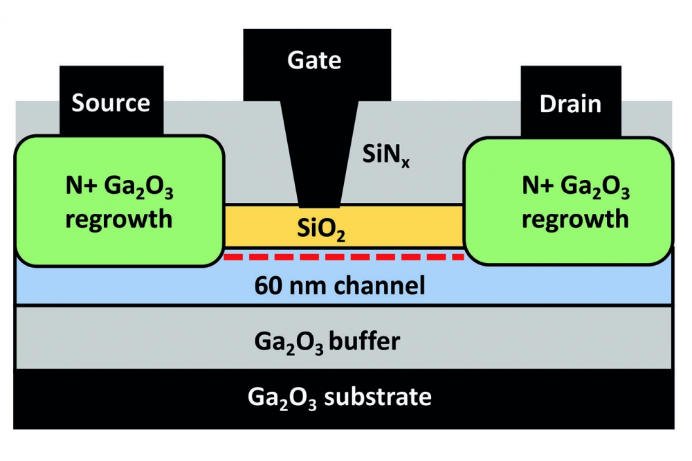
Fabrication of the team’s highly-scaled thin-channel MOSFETs, which employ a gate oxide to realise a higher breakdown voltage, began by loading a semi-insulating native substrate into an ozone MBE chamber. They used this reactor to grow a 200 nm-thick unintentionally doped buffer layer, followed by a 60 nm-thick silicon-doped channel. Plasma-enhanced atomic layer deposition provided a 20 nm-thick layer of SiO2 beneath a T-shaped Ni/Au gate, before regrowth by MOCVD added an n++ layer that provided the foundation for Ti/Au/Ni source and drain contacts added by electron-beam evaporation. Plasma-enhanced CVD of 200 nm-thick SiN ensured device passivation (see picture above).
DC measurements on one of the team’s β-Ga2O3 MOSFETs with a 175 nm gate length revealed an on-resistance of 23.7 Ω mm at a gate-source voltage of 6 V, a peak transconductance of 52 mS/m at a 10 V gate bias, and a maximum drain current of 285 mA mm-1 – that’s claimed to be comparable to the highest reported current density in Ga2O3 FETs.
The resistance at the interface between the re-growth layer and channel is estimated to be as high as 6.5 ± 0.6 Ω mm. This relatively large value could be due to atmospheric contaminants associated with the lack of pre-treatment, or may stem from the use of different epitaxial technologies. As fully MOCVD-grown MESFETs with low interface resistances have been reported, the team are not unduly concerned with this issue.
Biased at a gate-source voltage of -40 V, catastrophic breakdown of the MOSFETs occurred at 152 V, indicating a gate-drain breakdown voltage of 192 V and a 5.4 MV/cm average breakdown field.
High-frequency small signal measurements uncovered a record-breaking fmax of around 48 GHz and an ft of 11 GHz.
One of the team’s next goals to reduce the dimensions of its devices. “We plan to scale devices for more than 100 GHz fmax, and carry out large signal power measurements,” remarks Singisetti.
Reference
C.N. Saho et al. Appl Phys. Lett. 122 182106 (2023)


