
Advancing the InGaAs MOSFET
Offering greater ease of production over the HEMT, the InGaAs MOSFET is a promising candidate for very high frequency applications
Researchers from Taiwan have developed inversion-mode InGaAs MOSFETs that are claimed to produce outstanding values for transconductance and cut-off frequency (fT).
The work by the team at National Yang Ming Chiao Tung University should aid the development of sub-millimetre wave sources, which could be used in next-generation wireless communication networks and high-resolution imaging systems. According to the researchers, their transistors are an attractive alternative to GaAs-based and InP-based HEMTs that are widely used in RF applications, but are challenging to scale and require a complex epitaxial process for growth of the heterostructure.
III-V MOSFETs are said to address this concern, with those employing an InGaAs quantum-well delivering impressive results, including an ft of 370 GHz and a maximum cut-off frequency (fmax) of 400 GHz. “[But] in my opinion, quantum-well devices have an intricate epitaxial structure and complex fabrication processes,” argues team spokesman Jing-Yuan Wu, who points out that their inversion-mode devices, featuring a surface channel, have a simpler structure and benefit from fabrication with a CMOS-compatible process.
While the quantum-well variants have slightly higher performance than the MOSFETs produced by Wu and co-workers, the latter is claimed to have a higher commercial value – in terms of a lower cost, as well as ease of system-on-chip integration, which is a promising feature for the future.
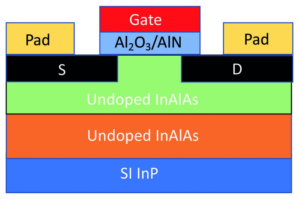
The team from Taiwan began the production of their transistors by loading 3-inch InP substrates into an MBE reactor and depositing a 100 nm-thick unintentionally doped InAlAs buffer, introduced to reduce signal loss, and a 50 nm-thick, lightly p-type doped In0.53Ga0.47As channel.
To produce devices from these epiwafers, the researchers removed the native oxide with diluted HCl, added a 10 nm Al2O3 cap by atomic layer deposition (ALD) that protected the In0.53Ga0.47As surface, and used photolithography to define the active area. They then added source and drain regions by silicon implantation and rapid thermal annealing, before applying diluted HF to remove the cap, using ALD to add an AlN interfacial passivation layer and an Al2O3 gate dielectric, before finally introducing contacts to this structure.
Wu and co-workers compared the performance of devices with gate lengths ranging from 75 nm to 400 nm. As expected, the drain current improved with scaling, rising threefold over this range of gate lengths to peak at 816 mA/mmm under gate and drain biases of 1.0V.
The peak transconductance for the transistor with the smallest gate length, realised at a drain-source voltage of 0.7 V, is 1035 mS mm-1. Using a drain-source voltage of 0.7 V and a gate-source voltage of 0.2 V, the team combined extrapolation with a small signal model to determine values for ftand fmax of 275 GHz and 75 GHz, respectively.
According to Wu, the low value for fmax is due to the very high resistance of the TiN gate stack. “To enhance fmax performance, we’ll try to introduce a gold-based alloy, which has low resistance.”
Values for the fT of the team’s transistor increase as the gate length decreases. Based on a TCAD simulation, they could hit 529 GHz at a 15 nm gate length.
Benchmarking with a metric that’s the product of ft and the gate length shows that the team’s devices outperform silicon and other InGaAs MOSFETs.
Wu and colleagues attribute this superiority to the excellent carrier transport properties of the In0.53Ga0.47As channel. Electron velocity in the channel is 2.88 x 107 cm s-1.
According to the team, their results show that the InGaAs MOSFET has great potential for future millimetre-wave and sub-terahertz applications.
Reference
J.-Y. Wu et al. Appl. Phys. Express 16 041007 (2023)


