
SiN trims the resistance of high-speed HEMTs
In-situ addition of SiN reduces the contact resistance of aluminium-rich HEMTs
Engineers from Xidian University, China, have significantly cut the contact resistance of GaN-based HEMTs with an aluminium-rich AlGaN barrier layer by in-situ insertion of SiN.
Their triumph promises to aid the development of HEMTs operating above 40 GHz. In these devices, the aluminium-rich AlGaN barrier enhances the transistor’s speed, but hampers the realisation of
a low contact resistance.
According to the team, their approach is simpler and cheaper than that of alternatives for realising high-frequency AlGaN/GaN HEMTs with a low contact resistance, such as silicon implantation and the re-growth of a heavily doped n-type GaN layer.
Spokesman for the researchers, Zhihong Liu, told Compound Semiconductor that the idea for inserting a SiN layer came from previous experimentals.
He remarked: “We knew that a thin layer of silicon, deposited in a certain way, could help the ohmic contact formation in GaN HEMTs; and at high temperatures the quality of SiN will degrade and become very leaky – so a thin layer of SiN may decompose and the remaining silicon help with the ohmic contact.”
Liu and co-workers investigated this possibility with an Al0.65Ga0.35N/GaN HEMT featuring a thin layer of SiN, grown in-situ on the surface of the heterostructure.
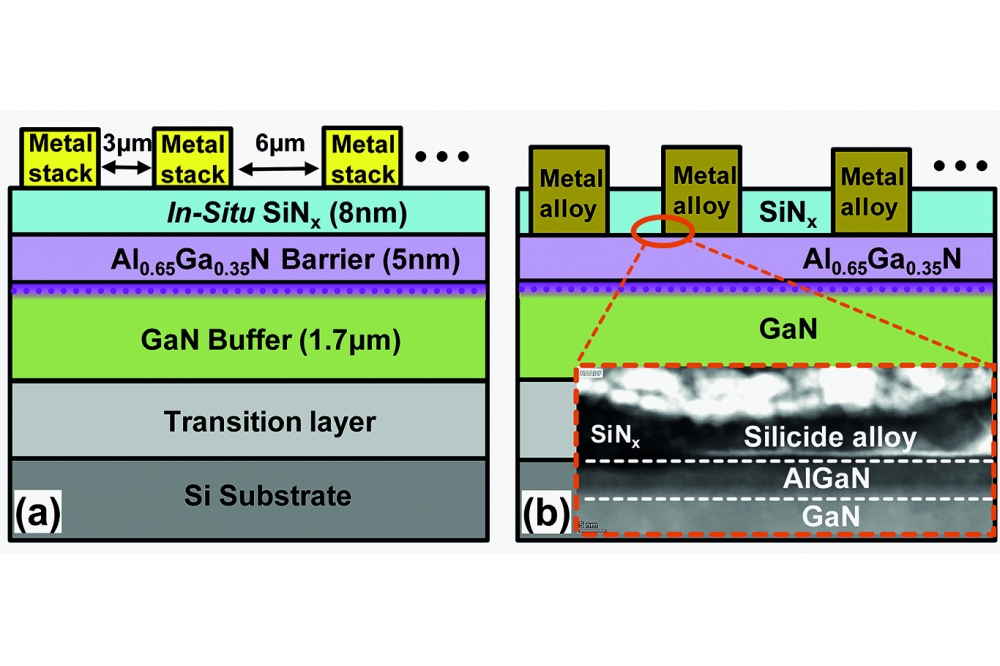
This study began by taking a sapphire substrate and growing, by MOCVD, a 1.7 mm-thick unintentionally doped GaN buffer, followed by a 5 nm-thick Al0.65Ga0.35N barrier and a 8 nm SiN layer. According to room-temperature Hall mobility measurements, this structure has a two-dimensional electron gas density of 2.2 x 1013 cm-2 and a mobility of 1190 cm2 V-1 s-1.
After planar isolation by argon-ion implantation, the team formed ohmic contacts through the addition of a Ti/Al/Ni/Au metal stack, annealed under nitrogen gas for 30 s at 850 °C. It is claimed that the composition of the stack and the annealing conditions is optimised. For comparison, the researchers fabricated a control, identical except for omission of the in-situ SiN layer.
Turning to the transfer length method, with electrode spacings from 3µm to 18 µm, revealed that adding of SiN reduced the contact resistance from 0.320 Ωmm to 0.175 Ω mm and cut the specific contact resistivity from 2.84 x 10⁻⁶ Ωcm2 to 8.45 x 10⁻⁷Ω cm2.
A combination of resistance-related measurements between 300 K and 450 K and modelling of this data allowed the team to deduce the primary transport mechanism in ohmic contacts at metal-semiconductor interfaces for both types of device.
That approach revealed that thermionic field emission governs transport in the ohmic contact of the sample with the SiN layer. This behaviour is beneficial in GaN-based electronic devices, because they often operate at high junction temperatures. In the control, field emission is thought to dominate, due to the thinness of the Al0.65Ga0.35N layer and its larger barrier height.
Inspecting the contacts with high-resolution transmission electron microscopy revealed that the 8 nm-thick SiN layer decomposed under annealing. It’s suggested that the dark clumps observed at the interface are TiN. They are partially surrounded by gold – its presence is confirmed energy-dispersive X-ray spectroscopy.
Liu admitted that he is still to optimise the thickness of the SiN layer, which has a tremendous impact on the resistance.
The team also applied its technology to an AlN/GaN HEMT, grown on silicon, and recorded high values for both the cut-off frequency and the maximum oscillation frequency. “This work is submitted to another journal and is still under review,” added Liu.
The next goals for the engineers are to try and improve the contacts by tuning the thickness of SiN, and using their recent breakthrough to develop millimetre-wave and terahertz HEMTs.
Reference
D. Hanghai et al. Appl. Phys. Lett. 121 172102 (2022)
Caption
After adding the metal contact to the heterostructure with a SiN layer (a), the annealing step creates a metal alloy that’s in contact with the Al0.65Ga0.35N barrier (b).


